Method for preparing flexible optical detector on basis of two-dimensional functional material

A photodetector and functional material technology, applied in the field of preparation of photodetectors, can solve the problems of difficult mass production and high cost of photolithography technology, and achieve high-density integration, good light transmission and small size Effect

Inactive Publication Date: 2012-09-12
HARBIN INST OF TECH
View PDF4 Cites 13 Cited by
  • Summary
  • Abstract
  • Description
  • Claims
  • Application Information

AI Technical Summary

Problems solved by technology

[0003] The present invention aims to solve the technical problems of the high cost of the photolithography process technology of the existing flexible phot

Method used


Image

  • Method for preparing flexible optical detector on basis of two-dimensional functional material
  • Method for preparing flexible optical detector on basis of two-dimensional functional material
  • Method for preparing flexible optical detector on basis of two-dimensional functional material

Examples


specific Embodiment approach 1

[0025] Embodiment 1: A method for preparing a flexible photodetector based on two-dimensional functional materials in this embodiment is carried out in the following steps:

[0026] 1. Synthesize semiconductor material single crystal gallium selenide or single crystal gallium sulfide by high temperature reaction in tube furnace;

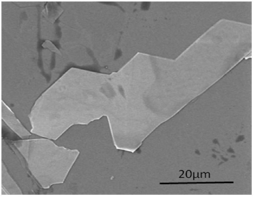
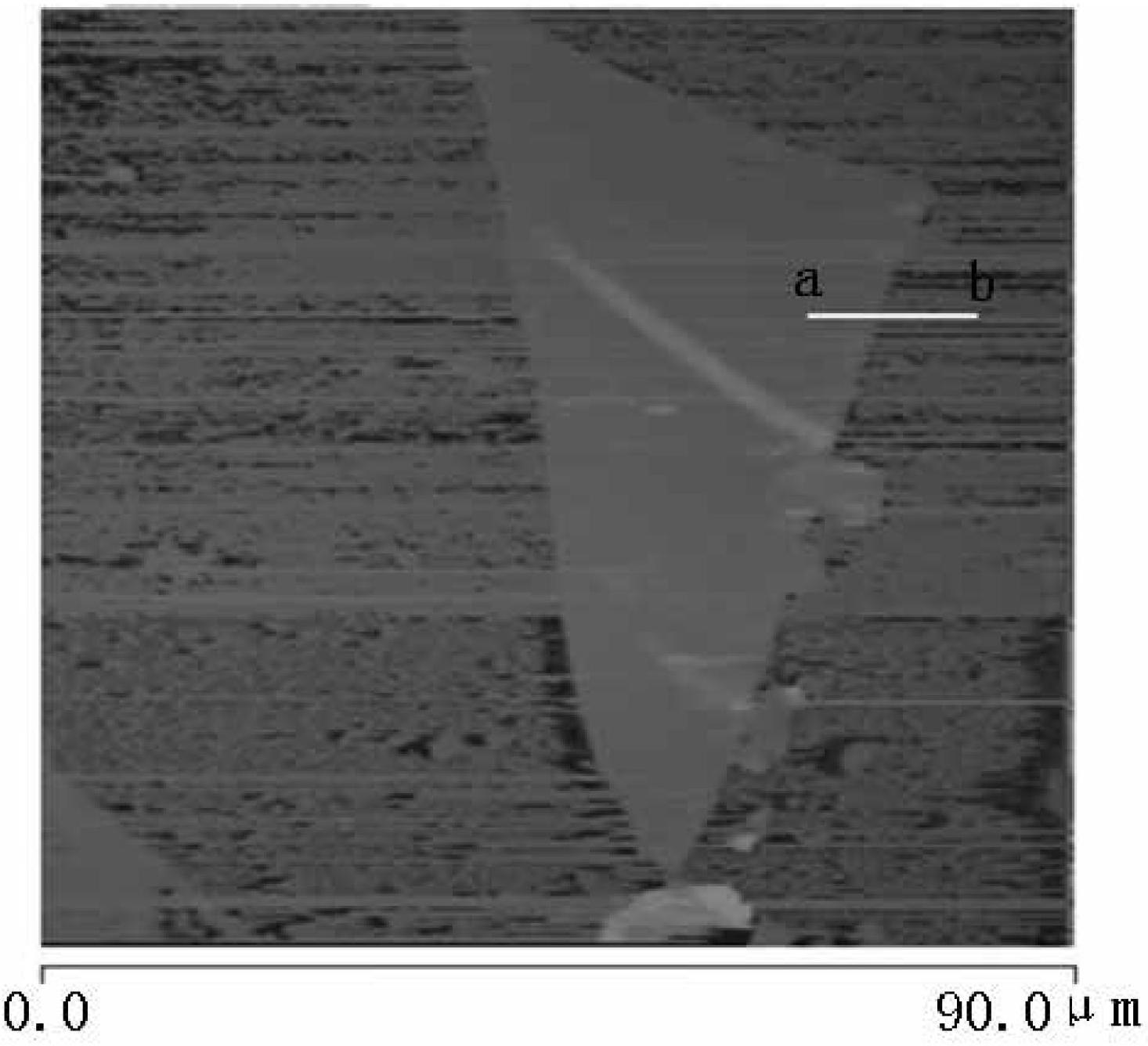
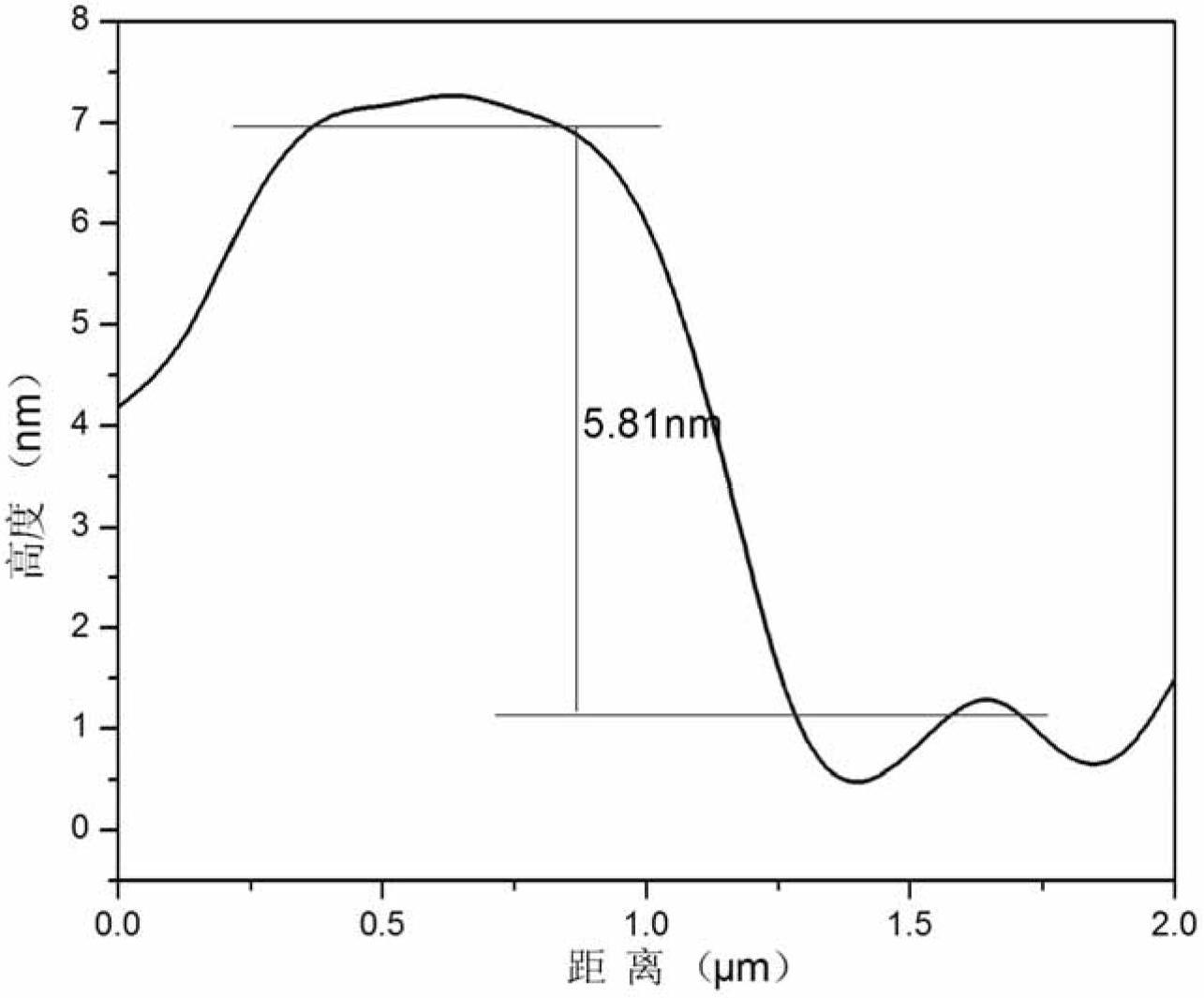
[0027] 2. Use Scotch tape to paste on the surface of the semiconductor material prepared in step 1—peel off 5 to 50 times to obtain a two-dimensional structure semiconductor material adhered to the Scotch tape;

[0028] 3. After cleaning the polyethylene terephthalate film substrate, stick the Scotch tape with the two-dimensional structure semiconductor material adhered to the polyethylene terephthalate plastic substrate obtained in step 2, and gently press it out The air bubbles between the tape and the substrate, after standing for 1 to 10 minutes, tear off the Scotch tape, wash the substrate with ethanol to remove the residual offset printing, and...

specific Embodiment approach 2

[0032] Specific embodiment two: the difference between this embodiment and specific embodiment one is that the preparation method of single crystal gallium selenide in step one is as follows: A, the molar ratio of gallium and selenium is 1: (1.3~2) and weighs analytical pure Gallium powder and analytically pure selenium powder are placed together in a tube furnace, wherein the selenium powder is located in the low temperature zone of the tube furnace, and the gallium powder is located in the high and low temperature zone of the tube furnace, and the gas flow rate is 10-30 sccm normal pressure argon Gas, the flow direction of argon is from the low-temperature area to the high-temperature area; B. Raise the temperature of the low-temperature area to 400-600 °C, and at the same time raise the temperature of the high-temperature area to 1000-1050 °C, and the selenium vapor contacts with the gallium along with the flow of argon gas And react, the reaction time is 30-45min; then the ...

specific Embodiment approach 3

[0033] Specific embodiment three: the difference between this embodiment and specific embodiment one is that the preparation method of single crystal gallium sulfide in step one is as follows: A, the molar ratio of gallium and sulfur is 1: (1.3~2) and weighs analytical pure gallium Powder and analytically pure sulfur powder are placed together in a tube furnace, wherein the sulfur powder is located in the low temperature zone of the tube furnace, and the gallium powder is located in the high and low temperature zone of the tube furnace, and the gas flow rate is 10-30 sccm normal pressure argon. , the flow direction of the argon is from the low temperature zone to the high temperature zone; B. Raise the temperature of the low temperature zone to 300-350°C, and at the same time raise the temperature of the high temperature zone to 1000-1050°C, the sulfur vapor comes into contact with the gallium along with the argon gas flow and A reaction occurs, and the reaction time is 30-45 m...


PUM

PropertyMeasurementUnit
Thicknessaaaaaaaaaa
Thicknessaaaaaaaaaa

Abstract

The invention discloses a method for preparing a flexible optical detector on the basis of the two-dimensional functional material, which relates to a preparation method for the optical detector. The method mainly aims to solve the technical problems that the conventional flexible optical detector has high photolithographic process technology cost and has difficulty in realizing mass production. The method comprises the following steps of: 1) preparing semiconductor materials, i.e. single crystal gallium selenide or single crystal gallium sulfide; 2) sticking and stripping on the surface of the semiconductor material by a scotch adhesive tape; 3) transferring the two-dimensional semiconductor material to a substrate; 4) covering a copper mask to the substrate processed in the step 3), depositing a gold metal layer and a chrome layer, removing the mask, and carrying out annealing processing; and 5) screening electrode couples with photoelectronic response to ultraviolet light in an optical detector semiconductor obtained in the step 4) to obtain the flexible optical detector prepared on the basis of the two-dimensional functional material. The ultraviolet light response degree of the optical detector is above 100AW<-1>. The flexible optical detector can be used as a microelectronic device and a photosensitive device to be used for the field of information transmission and storage.

Description

technical field [0001] The invention relates to a method for preparing a photodetector. Background technique [0002] The nano-semiconductor material with two-dimensional structure has unique electrical, optical, magnetic and mechanical properties, and this material is connected with modern high-tech micro-nano processing technology, which can well realize the high density of microelectronic devices and photosensitive devices Integration has great application potential in the electronics industry and energy conversion, and is expected to become the core material for next-generation information transmission and storage. With the development of electronic technology, the characteristic size of semiconductor devices has been continuously reduced, and gradually increased from micron to nanometer. Under the premise of ensuring the same electrical and optical functions, it is required to reduce the dimension of semiconductor materials used in devices. From the original The three-...

Claims


Application Information

Patent Timeline
IPC IPC(8): H01L31/18
CPCY02P70/50
Inventor 胡平安文振忠张荣福曹文武杨彬张甲王晓娜王立峰李晓超李俊杰
Owner HARBIN INST OF TECH
Why Eureka
Try Eureka