Infrared detector manufacturing method based on compound sacrificial layers

A technology of infrared detector and composite sacrificial layer, applied in the field of infrared detector, can solve the problems of peeling, inability to achieve planarization, poor adhesion of metal layer, etc.

Active Publication Date: 2014-11-05
ZHEJIANG DALI TECH
View PDF4 Cites 1 Cited by
  • Summary
  • Abstract
  • Description
  • Claims
  • Application Information

AI Technical Summary

Problems solved by technology

Therefore, the detector manufacturing process using the polyimide sacrificial layer process cannot be fully compatible with CMOS production
However, the dielectric sacrificial layer is often deposited on the surface of CMOS, which cannot achieve the function of planarization; or there are shortcomings such as poor adhesion to the metal layer on the substrate surface, which will cause peeling in the subsequent process.

Method used


Image

  • Infrared detector manufacturing method based on compound sacrificial layers
  • Infrared detector manufacturing method based on compound sacrificial layers
  • Infrared detector manufacturing method based on compound sacrificial layers

Examples


Embodiment 1

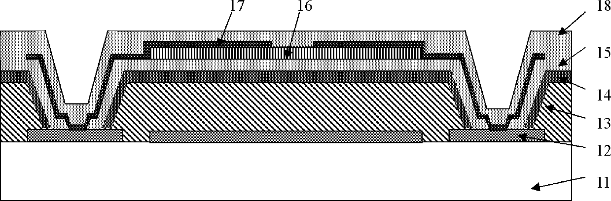
[0068] Figure 2 is figure 1 The flow chart of the first processing method of the infrared detector is shown. The infrared detector processing method of the present invention will be described in detail below in conjunction with FIG. 2 , and the present invention will be further described.

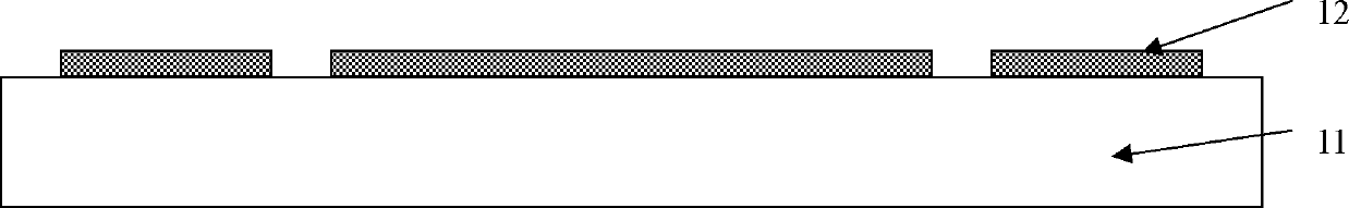
[0069] 2(a), fabricating and patterning the metal layer 12 on the substrate 11 to form an infrared reflection layer and an electrical connection with CMOS. Wherein, the substrate 11 is a silicon wafer that has been processed with CMOS circuits. One of Ti / TiN / Al (alloy including Al), TiW / Al (alloy including Al), and Ta / TaN / Al (alloy including Al) is used for the metal reflective layer 12 . The thickness of the control metal layer 12 is between 1000A~10000A.

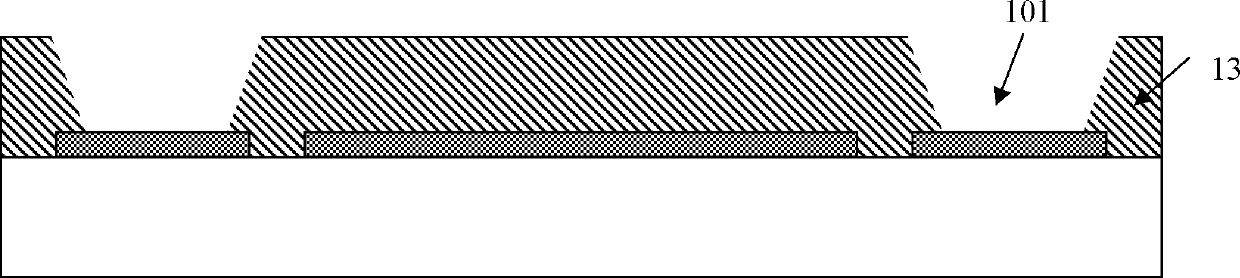
[0070] 2(b), making a first sacrificial layer 13 of polyimide on the metal layer 12, which is prepared by a spin-coating method. In this embodiment, the polyimide is photosensitive, and through-holes 101 are formed by exposure and d...


PUM


Abstract

The invention discloses a method utilizing compound sacrificial layers to manufacture an infrared detector. The method comprises sequentially enabling a metal layer, a first polyimide sacrificial layer, a second amorphous silicon sacrificial layer and through holes formed by imaging of the sacrificial layers to be arranged on a complementary metal-oxide-semiconductor (CMOS) silicon substrate; in a laminating mode, manufacturing a structure layer and contact holes formed by imaging; manufacturing a sensitive layer, a metal electrode layer and a release protecting layer, and imaging the sensitive layer, the electrode layer and a microbridge structure. When the sacrificial layers are released, first the second sacrificial layer is released, and then the first sacrificial layer is released. Compared with the prior art, the infrared detector manufacturing method effectively enables two kinds of different sacrificial layers to be effectively utilized, the organic sacrificial layer can be utilized to carry out planarization on the surface of a CMOS, the adhesion between the surface of the CMOS and metal is improved, and the inorganic sacrificial layer is utilized to control volatility of polyimide so as to be more compatible with the CMOS process.

Description

technical field [0001] The invention relates to the field of infrared detectors, in particular to an uncooled infrared detector processing method using different materials to form a composite sacrificial layer. Background technique [0002] Uncooled infrared detectors have been used in various military and civilian fields, such as automotive night vision systems, weapon sights, power testing instruments, and crowd monitoring facilities in important places, due to their advantages of working at room temperature, light size, and relatively low cost. etc. are widely used. [0003] At present, the mainstream uncooled infrared detector is Microbolometer (Microbolometer) technology, which is a device that combines CMOS readout circuit and microelectromechanical system (MEMS) processing. The commonly used structure is to manufacture a heat-insulating micro-bridge structure integrated with the CMOS substrate monomer by using the surface micromachining process of the sacrificial lay...

Claims


Application Information

Patent Timeline
Patent Type & Authority Patents(China)
IPC IPC(8): H01L31/18
CPCY02P70/50
Inventor 姜利军池积光钱良山罗雯雯
Owner ZHEJIANG DALI TECH
Why Eureka
Try Eureka