Electrode magnetron sputtering process of NTC temperature sensor

A temperature sensor, magnetron sputtering technology, applied in thermometers, sputtering plating, metal material coating processes, etc. High density, uniform particle size and good adhesion

Inactive Publication Date: 2012-09-26
XINGHUA XINXING ELECTRONICS
View PDF4 Cites 1 Cited by
  • Summary
  • Abstract
  • Description
  • Claims
  • Application Information

AI Technical Summary

Problems solved by technology

[0002] The electrode material of the existing NTC temperature sensor chip is silver, and the process method is printing. Its defects: electrode thickness>1μm, and thickness error>±20%, resulting in product resistance accuracy>±5%
Affected by the environmental conditions of use such as humidity and corrosive gases, the electrode silver ions will migrate, resulting in deterioration of product performance, reliability and stability

Method used


Image

  • Electrode magnetron sputtering process of NTC temperature sensor
  • Electrode magnetron sputtering process of NTC temperature sensor

Examples


Embodiment 1

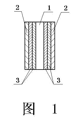
[0015] An NTC temperature sensor magnetron sputtering electrode process, including the following process steps: using a semiconductor sensitive ceramic substrate 1 with a thickness of 0.3mm, a length of 0.5mm, and a width of 0.5mm, the surface of the semiconductor sensitive ceramic substrate 1 is cleaned as follows : Soak and ultrasonically clean the semiconductor sensitive ceramic substrate 1 in a deionized aqueous solution, then soak the semiconductor sensitive ceramic substrate 1 in a high-purity IPA solution to remove surface stains, ultrasonically clean for 5 minutes, and finally rinse with ionized water, heat and bake the semiconductor sensitive ceramic substrate 1 Dry standby, temperature control 200±10℃;

[0016] Magnetron sputtering: Place the above semiconductor sensitive ceramic substrate 1 in the vacuum chamber of the multi-target facing target magnetron sputtering equipment, use argon gas with a mass purity of 99.99% as the working gas, and the working vacuum degre...

Embodiment 2

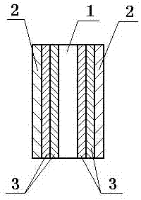
[0018] A magnetron sputtering electrode process for an NTC temperature sensor, comprising the following process steps: using a semiconductor sensitive ceramic substrate 1 with a thickness of 1 mm, a length of 2.5 mm, and a width of 2.5 mm, the surface of the semiconductor sensitive ceramic substrate 1 is cleaned as follows: Soak in deionized aqueous solution for ultrasonic cleaning, then soak the semiconductor sensitive ceramic substrate 1 in absolute ethanol solution to remove surface stains, ultrasonically clean for 5 minutes, and finally rinse with ionized water, heat and dry the semiconductor sensitive ceramic substrate 1 Standby, temperature control 200±10℃;

[0019] Magnetron sputtering: Place the above semiconductor sensitive ceramic substrate 1 in the vacuum chamber of the multi-target facing target magnetron sputtering equipment, use argon gas with a mass purity of 99.99% as the working gas, and the working vacuum degree is 0.1-1 Pa, the sputtering distance is 80-120m...


PUM

PropertyMeasurementUnit
thicknessaaaaaaaaaa
thicknessaaaaaaaaaa
thicknessaaaaaaaaaa

Abstract

The present invention discloses an electrode magnetron sputtering process of an NTC temperature sensor, and the process comprises the following process steps of: (1) conducting cleaning treatment on the surface of a semiconductor sensitive ceramic substrate, then performing heating and drying for standby use, with the temperature controlled at 190-210DEG C; (2) carrying out magnetron sputtering: putting the semiconductor sensitive ceramic substrate in the vacuum chamber of a multi-target facing target magnetron sputtering device, employing different target materials respectively to implement target material deposition on the semiconductor sensitive ceramic substrate, thus making a transition layer and an electrode film layer attached to the surface of the semiconductor sensitive ceramic substrate in order. The NTC temperature sensor made by the process of the invention has high density and resistance precision, uniform thickness, and is exempt from environmental influence, and no electrode ion migration can occur, so that product reliability and stability are greatly improved.

Description

technical field [0001] The invention belongs to temperature sensor technology, in particular to a production process for preparing temperature sensor electrodes by magnetron sputtering against a target. Background technique [0002] The electrode material of the existing NTC temperature sensor chip is silver, and the process method is printing. Its defects are: electrode thickness > 1 μm, and thickness error > ± 20%, resulting in product resistance accuracy > ± 5%. Chinese patent 200410074623.X discloses a soft ferrite magnetic core magnetron sputtering vacuum silver plating method, at first the soft ferrite magnetic core is placed in a vacuum furnace for heating, and it is characterized in that it also includes the following steps: a. Use a stainless steel target at a bias voltage of 300-400V to bombard and clean the soft ferrite core; b. Use a stainless steel target at a negative bias of 50-80V to plate a transition layer of 0.5-1 microns on the soft ferrite cor...

Claims


Application Information

Patent Timeline
Patent Type & Authority Applications(China)
IPC IPC(8): C23C14/35C23C14/18G01K7/22
Inventor 刘英
Owner XINGHUA XINXING ELECTRONICS
Why Eureka
Try Eureka