Grating coupler and manufacturing method thereof

A technology of a grating coupler and a manufacturing method, which is applied to the coupling of optical waveguides, light guides, optics, etc., can solve the problem that the grating coupler is not suitable for integration in CMOS technology, the coupling efficiency of the grating coupler is difficult to improve, and the thickness of the SOI buried oxide layer is strictly required. and other problems, to achieve the effect of relaxing specification requirements, reducing dependence, and reducing production costs

Active Publication Date: 2012-09-26
SHANGHAI INST OF MICROSYSTEM & INFORMATION TECH CHINESE ACAD OF SCI
View PDF8 Cites 10 Cited by
  • Summary
  • Abstract
  • Description
  • Claims
  • Application Information

AI Technical Summary

Problems solved by technology

[0005] In view of the shortcomings of the prior art described above, the purpose of the present invention is to provide a grating coupler and its manufacturing method, which are used to solve the problem that the coupling efficiency of the grating c

Method used


Image

  • Grating coupler and manufacturing method thereof
  • Grating coupler and manufacturing method thereof
  • Grating coupler and manufacturing method thereof

Examples


Embodiment 1

[0044] Such as Figure 1~5 As shown, the present embodiment provides a method for manufacturing a grating coupler, and the method at least includes the steps of:

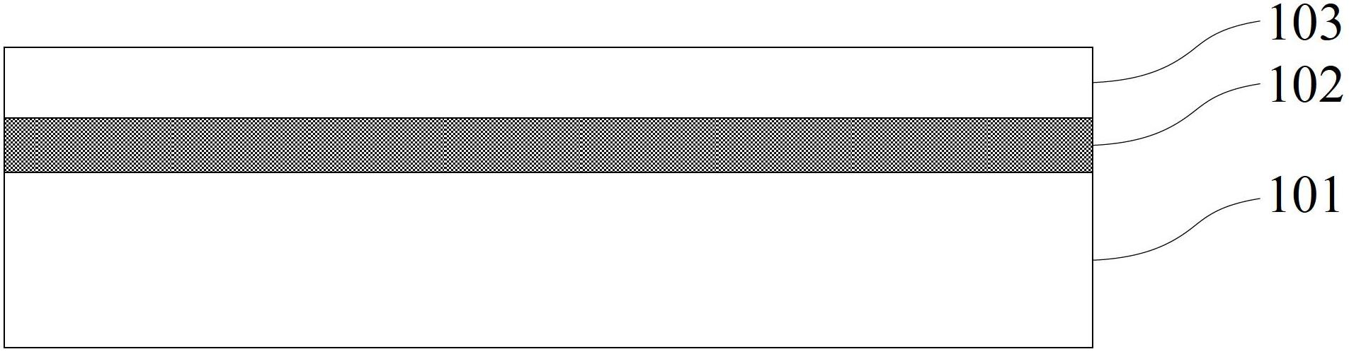
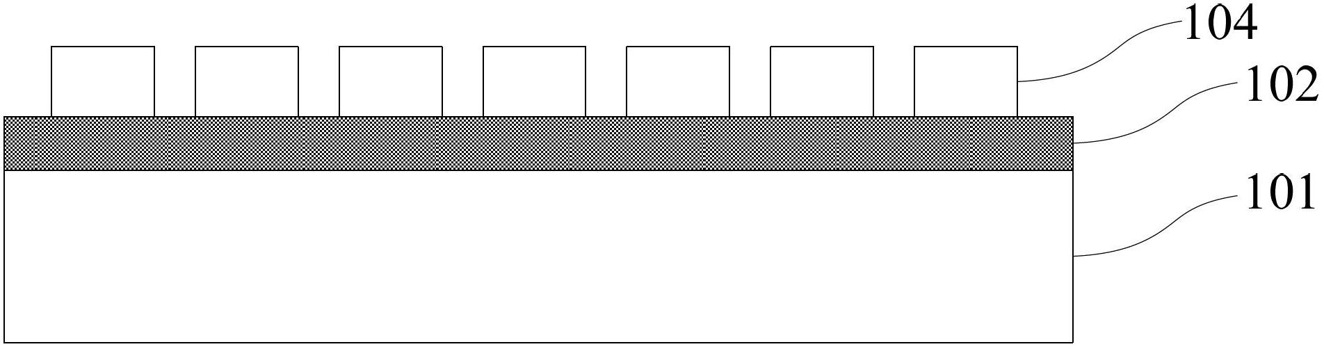
[0045] Such as Figure 1~2As shown, step 1) is first performed, providing an SOI substrate, the SOI substrate includes a back substrate 101, a buried oxide layer 102, and a top layer of silicon 103, and etching the top layer of silicon 103 to the buried oxide layer 102, A coupling grating 104 having a plurality of silicon block structures arranged at intervals and a period of 500-800 nm is formed.

[0046] The ratio of the width of the silicon block structure to the period of the coupling grating 104 is 0.7-0.99:1. In this embodiment, the ratio of the width of the silicon block structure to the period of the coupling grating 104 is 0.9:1, that is, the filling factor of the coupling grating 104 is 0.9. Specifically, if the period of the coupling grating 104 is selected as 700nm, the width of the silicon block stru...

Embodiment 2

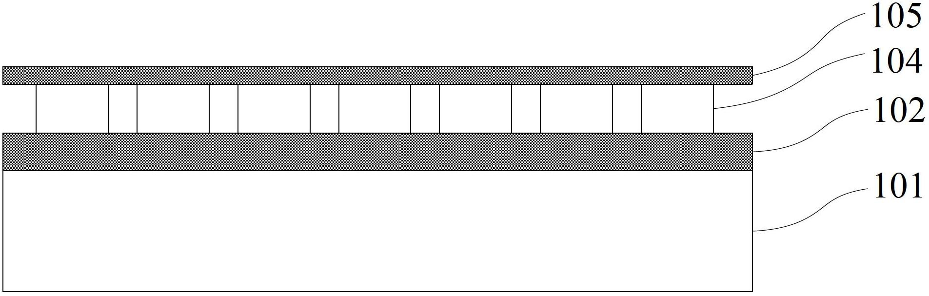
[0062] see Figure 6~Figure 10 , as shown in the figure, this embodiment provides a method for fabricating a grating coupler, such as Figure 1~5 As shown, the present embodiment provides a method for manufacturing a grating coupler, and the method at least includes the steps of:

[0063] Such as Figure 6~7 As shown, step 1) is first performed, providing an SOI substrate, the SOI substrate includes a back substrate 101, a buried oxide layer 102, and a top layer of silicon 103, and etching the top layer of silicon 103 to the buried oxide layer 102, A coupling grating 104 with a plurality of silicon block structures arranged at intervals and a period of 500-800 nm is formed, and at least one CMOS active region 108 with shallow trench isolation grooves 109 on both sides is isolated in the top layer of silicon 103 .

[0064] In this embodiment, a pattern including etching the coupling grating 104 and one or more CMOS active regions 108 is produced in the same mask, and the top-...


PUM

PropertyMeasurementUnit
Thicknessaaaaaaaaaa
Thicknessaaaaaaaaaa
Widthaaaaaaaaaa

Abstract

The invention provides a grating coupler and a manufacturing method thereof. The manufacturing method comprises the following steps of: providing an SOI (Silicon On Insulator) substrate and etching top-layer silicon of the SOI substrate to form a coupling grating with the period of 500-800 nm; meanwhile, separating a CMOS (Complementary Metal-Oxide-Semiconductor Transistor) active region in the top-layer silicon; manufacturing a grating oxidizing layer covering the coupling grating and the CMOS active region on the coupling grating; forming a conductive layer on the surface of the grating oxidizing layer and etching the conductive layer to form a coating structure which has the same period as the coupling grating; meanwhile, forming a gate structure of a CMOS; and finally, forming a protection layer to finish the preparation. The preparations of the coupling grating, the grating oxidizing layer, the coating structure and the CMOS can be simultaneously finished and a mask can be shared, so that the manufacturing cost is reduced; the coupling efficiency is improved by an upper conductive coating covering the grating oxidizing layer; the coupling efficiency of the grating coupler is obviously improved by optimized structure parameters; and the dependency of the coupling efficiency on the thickness of an SOI buried oxide layer is greatly reduced by a novel grating coupler structure, so that the specification requirements on the SOI substrate are reduced.

Description

technical field [0001] The invention belongs to the field of semiconductors and optoelectronic integration, and in particular relates to a grating coupler and a manufacturing method thereof. Background technique [0002] Integrated silicon-based optical systems, due to their small device size and good compatibility with traditional integrated circuit CMOS processes, have become a hot research topic at present. Many micro-nano devices have been integrated on silicon, such as lasers, modulators, filters, couplers, buffers, etc. The grating is used to realize the function of the coupler, which has the advantages of small coupling area and high coupling efficiency, so it is widely used in planar optical systems. [0003] Si and SiO 2 The high refractive difference (about 2.0) provides the possibility to realize nano-optical waveguides and ultra-small-scale integrated optical waveguide devices, and has great application prospects in the fields of optical communication, optical ...

Claims


Application Information

Patent Timeline
IPC IPC(8): G02B6/34G02B6/124G02B6/136
Inventor 盛振仇超甘甫烷武爱民王曦邹世昌
Owner SHANGHAI INST OF MICROSYSTEM & INFORMATION TECH CHINESE ACAD OF SCI
Why Eureka
Try Eureka