Measurement system and measurement method of secondary electron emission yield of dielectric material

A technology of secondary electron emission and dielectric materials, applied in the space application field of aerospace materials, can solve the problems of complex measurement, influence, limited experimental accuracy and efficiency, and achieve high measurement efficiency, avoiding direct errors and small errors.

Inactive Publication Date: 2012-10-03
BEIJING INST OF SPACECRAFT ENVIRONMENT ENG
View PDF7 Cites 22 Cited by
  • Summary
  • Abstract
  • Description
  • Claims
  • Application Information

AI Technical Summary

Problems solved by technology

[0002] Existing methods for measuring the secondary electron emission coefficient of dielectric materials generally use ion beams or ultraviolet radiation to eliminate the charge on the surface of the sample, and then measure the secondary electron emission coefficient after treatment. However, this measurement method not only makes the measurement Complicated, with limited experimental precision and efficiency
For example, Chinese patent application CN201010617890.2 "A test device for distinguishing material secondary electrons and backscattered electrons" discloses a test device for distinguishing material secondary electrons and backscattered electrons. The device includes a light bar, a Faraday cup, Current collector, insulating pad, retardation grid and sample stage, this device can distinguish secondary electrons and backscattered electrons generated after the interaction between primary electrons and materials, and also has the function of analyzing the energy spectrum of secondary electrons and backscattered electrons, However, in the secondary electron measurement process, the incident electron beam charges the sample, and the surface potential of the sample will further affect the actual energy of the incident electrons reaching the sample surface. Therefore, the "secondary electron yield - incident electron energy" to be measured will be Curves make a difference

Method used


Image

  • Measurement system and measurement method of secondary electron emission yield of dielectric material
  • Measurement system and measurement method of secondary electron emission yield of dielectric material

Examples


Embodiment Construction

[0019] The following is a specific implementation manner of the content of the present invention, and the content of the present invention will be further clarified through the specific implementation mode below. Of course, the following specific embodiments are described only to illustrate different aspects of the present invention, and should not be construed as limiting the scope of the present invention.

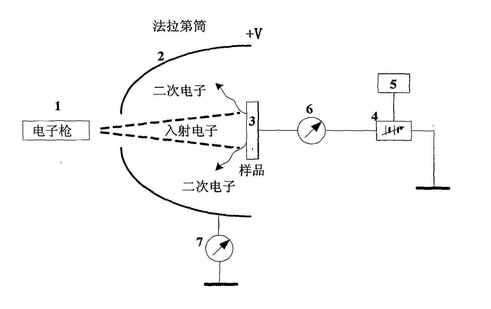
[0020] refer to figure 1 , figure 1 It is a schematic diagram of the structure of the measurement system for the secondary electron emission coefficient of the dielectric material of the present invention. Wherein, the measurement system of the secondary electron emission coefficient of the dielectric material of the present invention includes a Faraday cup and a pulsed electron gun, wherein the Faraday cup is provided with an electron entrance, and the Faraday cup can be used to collect samples under a positive bias of about ten volts. For the generated secondary elec...


PUM


Abstract

The invention discloses a measurement system and a measurement method of a secondary electron emission yield of dielectric material. The measurement system comprises a Faraday cup and a pulse electron gun, wherein an incident beam generated by the pulse electron gun outside the Faraday cup irradiates on a sample through an electronic entrance port on a tube, and an automatic voltage regulator circuit is electrically connected between a sample back electrode and an earth wire, so that the level on the sample surface is kept constant relative to a potential difference between the electron guns. The voltage regulating range of the voltage adjustor circuit is controlled by a feedback control circuit in real time, so as to ensure that charging potential of the sample is compensated in real time, and current probes for measuring net collection current and secondary electron current are respectively connected between the sample and a voltage controlled power source of the voltage regulator circuit, and connected with the Faraday cup. According to the measurement system and the method disclosed by the invention, are simple extra consumer power equipment such as an ion source and the like and related experimental links are not needed, the measurement efficiency is high, and the measurement is continuous without stopping to carry out work such as energy dissipation, surface level measurement and the like after each irradiation pulse, and the measurement error is small.

Description

technical field [0001] The invention belongs to the technical field of space application of aerospace materials, and in particular relates to a measurement system and a measurement method of a secondary electron emission coefficient. Background technique [0002] Existing methods for measuring the secondary electron emission coefficient of dielectric materials generally use ion beams or ultraviolet radiation to eliminate the charge on the surface of the sample, and then measure the secondary electron emission coefficient after treatment. However, this measurement method not only makes the measurement Complicated, and the experimental precision and efficiency are limited. For example, Chinese patent application CN201010617890.2 "A test device for distinguishing material secondary electrons and backscattered electrons" discloses a test device for distinguishing material secondary electrons and backscattered electrons. The device includes a light bar, a Faraday cup, Current co...

Claims


Application Information

Patent Timeline
Patent Type & Authority Applications(China)
IPC IPC(8): G01N23/22
Inventor 黄建国易忠刘业楠孟立飞张超王志浩唐小金徐焱林陈金刚邓佳欣
Owner BEIJING INST OF SPACECRAFT ENVIRONMENT ENG
Why Eureka
Try Eureka