Array substrate, manufacturing method thereof, display panel and display device

An array substrate and manufacturing method technology, applied in the field of liquid crystal display, can solve the problems of high manufacturing cost of the array substrate, achieve the effect of increasing aperture ratio, flexible process conditions, and micro-controllable device characteristics

Active Publication Date: 2013-07-03
BOE TECH GRP CO LTD +1
View PDF5 Cites 0 Cited by
  • Summary
  • Abstract
  • Description
  • Claims
  • Application Information

AI Technical Summary

Problems solved by technology

[0006] It can be seen that the above-mentioned manufacturing process of the array substrate includes six patterning processes, and a different mask is used in each patterning process, resulting in a relatively high manufacturing cost of the array substrate.

Method used


Image

  • Array substrate, manufacturing method thereof, display panel and display device
  • Array substrate, manufacturing method thereof, display panel and display device
  • Array substrate, manufacturing method thereof, display panel and display device

Examples


Embodiment Construction

[0046] In order to make the object, technical solution and advantages of the present invention clearer, the present invention will be described in detail below with reference to the accompanying drawings and specific embodiments.

[0047] refer to Figure 9 , the manufacturing method of the array substrate according to the embodiment of the present invention may include the following steps:

[0048] Step 91, forming gate electrodes and gate lines on the substrate;

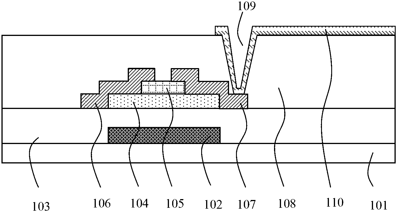
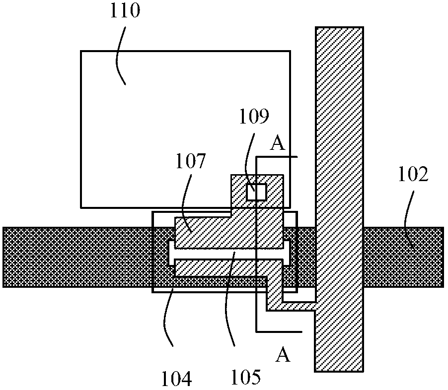
[0049] Such as figure 2 As shown, first, sputtering, thermal evaporation or other film forming methods can be used to form a gate metal layer on the glass substrate 101 or other types of transparent substrates. The gate metal layer can be made of chromium (Cr), molybdenum (Mo), aluminum (Al), copper (Cu), tungsten (W), neodymium (Nd), indium zinc oxide (IZO), indium tin oxide (ITO) and their alloys, and the gate metal layer can be one or more layers Then, a photoresist is formed on the gate metal layer; secondl...


PUM


Abstract

Provided are an array substrate, a manufacturing method thereof, a display panel, and a display device. The array substrate comprises: an etching stop layer (501) that is formed on a substrate (101) formed with an active layer and has a source electrode contact hole (502) and a drain electrode contact hole (503); a source electrode, a drain electrode, and a data line that are formed on the substrate formed with the etching stop layer (501), the source electrode being connected to the active layer through the source electrode contact hole (502), and the drain electrode being connected to the active layer through the drain electrode contact hole (503); a passivation layer (701) that is formed on the substrate formed with the source electrode, the drain electrode, and the data line and has a pixel electrode contact hole, the orthographic projection of the pixel electrode contact hole on the substrate (101) coinciding with the orthographic projection of the drain electrode contact hole (503) on the substrate; and a pixel electrode formed on the substrate formed with the passivation layer (701), the pixel electrode (801) being connected to the drain electrode through the pixel electrode contact hole. The present invention can reduce the manufacturing cost of the array substrate.

Description

technical field [0001] The invention relates to the field of liquid crystal display, in particular to an array substrate, a manufacturing method thereof, a display panel and a display device. Background technique [0002] The disadvantage of using amorphous silicon (a-Si) thin film transistors (TFTs) to make TFT displays is their very low electron mobility (<1cm 2 / V.S), and a-Si is opaque in the visible light range and has strong photosensitivity, so its application range is limited. With the emergence of new technologies, such as organic light-emitting diode (OLED) display technology, transparent liquid crystal display technology, and driver circuit integrated glass technology (Gate Driver on Array, GOA), etc. Electron mobility, better amorphous uniformity, and the ability to reduce threshold voltage (Vth) drift, etc. [0003] The metal oxide semiconductor thin film of metal oxide semiconductor thin film transistor (Oxide TFT, O-TFT) has low deposition temperature, hi...

Claims


Application Information

Patent Timeline
Patent Type & Authority Patents(China)
IPC IPC(8): H01L29/786H01L27/02H01L21/77
CPCG02F2001/136231H01L31/115G02F1/135H01L27/1248H01L29/7869H01L27/1225G02F1/136231
Inventor 杨玉清朴承翊李炳天蒋冬华
Owner BOE TECH GRP CO LTD
Why Eureka
Try Eureka