A method for forming a packaging pattern

A pattern and integrated circuit technology, which is applied in the field of packaging pattern formation, can solve the problems of low adhesion between the molecules in the lower layer of the packaging pattern and the substrate molecules, and the high viscosity of the packaging pattern.

Active Publication Date: 2015-09-30
CHIPMORE TECH CORP LTD
View PDF4 Cites 0 Cited by
  • Summary
  • Abstract
  • Description
  • Claims
  • Application Information

AI Technical Summary

Problems solved by technology

[0005] However, the packaging pattern obtained by the above method is relatively viscous, the adhesion between the molecules in the lower layer of the packaging pattern and the substrate molecules is small, and there is a gap between the packaging pattern and the substrate, such as figure 1 As shown, it is easy to cause the bumps prepared in the subsequent process to be interconnected

Method used


Image

  • A method for forming a packaging pattern
  • A method for forming a packaging pattern
  • A method for forming a packaging pattern

Examples


preparation example Construction

[0039] In the present invention, there is no special limitation on the preparation method of the above-mentioned substrate. It is preferably a composite substrate made of Si, and the thickness of the substrate is preferably 100-1000 um, more preferably 200-800 um, and most preferably 725 um.

[0040] The step b) specifically includes: spin-coating an organic photoresist solution on the substrate at a speed of 5-45 r / s, and baking at 90-150° C. for 2-8 minutes to obtain a photoresist film. The spin coating speed is preferably 25-45 r / s, more preferably 35 r / s. The above-mentioned baking temperature is preferably 90 to 120°C, more preferably 105°C. The above baking time is preferably 2.5 to 6 minutes, more preferably 3 to 4 minutes. The organic solution of the photoresist preferably has a propylene resin concentration of 20%-30%, a multifunctional acrylate (or fat) concentration of 10%-20%, and a photosensitizer content of 5%-15%. The thickness of the photoresist film obtained...

Embodiment 1

[0046] a) The Si substrate substrate is cleaned with deionized water for 2 minutes, blown dry with nitrogen gas, and dried in an oven.

[0047] b) Spin-coat THB121N photoresist (photosensitizer content 5%-15%) of JSR Company on the substrate at a speed of 35r / s, and bake the glue on a hot stage at 105°C for 200 seconds to obtain a 20 micron photoresist. photoresist film;

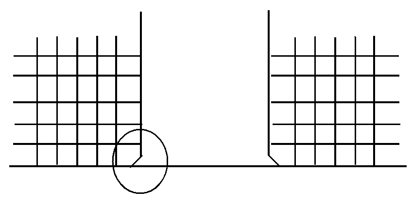
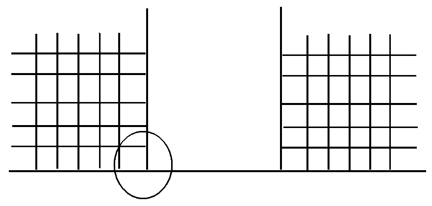
[0048] c) Exposure of the photoresist film to an exposure energy of 300mj / cm 2 Expose to ultraviolet light for 90 seconds, develop at 23°C for 90 seconds, wash with water, spin dry, and expose to obtain multiple cuboid-shaped preforms;

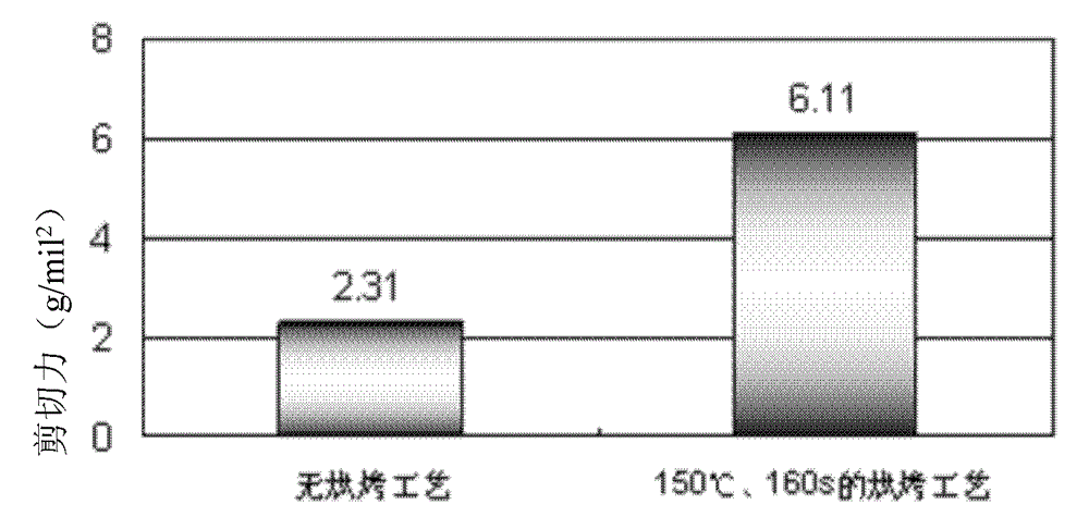
[0049] d) Bake the multiple preforms obtained in step c) at 150°C for 110 seconds;

[0050] e) The product obtained in step d) is subjected to an exposure energy of 660mj / cm 2 The ultraviolet light was exposed for 60 seconds, and then baked at 140° C. for 25 minutes, and the baked product was bombarded with oxygen plasma for 1 minute.

Embodiment 2

[0052] The baking time is 160 seconds in step d), and all the other are identical with embodiment 1.


PUM

PropertyMeasurementUnit
thicknessaaaaaaaaaa
adhesivityaaaaaaaaaa

Abstract

The invention provides a forming method of a packaging pattern. The method includes the following steps of: providing a substrate; spinning an organic solution of a photoresist on the substrate and drying to obtain a photoresist film; presetting an exposure shape, and conducting ultraviolet light exposure on the photoresist film to from a number of prefabricated bodies; baking the prefabricated bodies; and conducting ultraviolet light exposure, baking treatment and plasma treatment on the above obtained products. Compared with a prior art, the method of the invention employs baking treatment on the prefabricated bodies to volatilize water in the photoresist, reduce viscosity of the photoresist, and enhance intermolecular force of the photoresist and acting force between the photoresist molecules and the substrate, so that the formed package pattern gains large adhesion to closely contact on the substrate, thereby avoiding gap between the package pattern and the substrate and interconnection of bumps prepared in subsequent processes. Experimental results show that the package pattern formed by the method of the invention has adhesion of 6.54g / mil<2>.

Description

technical field [0001] The present invention relates to the technical field of semiconductor manufacturing, and more specifically, to a method for forming packaging patterns. Background technique [0002] With the continuous development of integrated circuit technology, electronic products are increasingly developing in the direction of miniaturization, intelligence, high performance and high reliability. Integrated circuit packaging means long bumps on the input and output pins of VLSI, which not only directly affects the performance of integrated circuits, electronic templates and even the whole machine, but also restricts the miniaturization, low cost and low cost of the entire electronic system. Reliability, including: sputtering metal process, photolithography process, bump process, etching process and inspection process, etc. [0003] Photolithography plays a pivotal role in the manufacturing process of semiconductor integrated circuits. Before performing ion implant...

Claims


Application Information

Patent Timeline
Patent Type & Authority Patents(China)
IPC IPC(8): G03F7/20G03F7/38G03F7/40H01L21/00
Inventor 张贤亮孙彬
Owner CHIPMORE TECH CORP LTD
Why Eureka
Try Eureka