

Strained SiGe BiCMOS (bipolar complementary metal oxide semiconductor) integrated device and preparation method
A technology for integrating devices and devices, which is applied in the field of strained SiGe BiCMOS integrated devices and its preparation, which can solve problems such as unsatisfactory photolithography technology, difficulty in meeting the design of Si-based process devices, and affecting device performance.
- Summary
- Abstract
- Description
- Claims
- Application Information
AI Technical Summary
Problems solved by technology
Method used
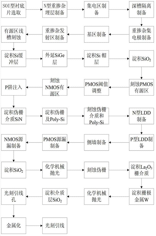
Image

Examples
Embodiment 1
[0089] Embodiment 1: The strained SiGe BiCMOS integrated device and the circuit that the channel length is prepared are 22nm,
[0090] Specific steps are as follows:
[0091] Step 1, epitaxial growth.
[0092] (1a) Select the SOI substrate, the support material of the lower layer of the substrate is Si, and the middle layer is SiO 2 , with a thickness of 150nm, and the upper material is doped with a concentration of 1×10 16 cm -3 N-type Si with a thickness of 100nm;
[0093] (1b) Thermally oxidize a layer of SiO with a thickness of 300nm on the substrate surface 2 layer;
[0094] (1c) Lithograph the buried layer region, implant N-type impurities into the buried layer region, and anneal at 800°C for 90 minutes to activate the impurities to form an N-type heavily doped buried layer region (impurity concentration ≥ 10 20 cm -3 ).
[0095] Step 2, isolation area preparation.
[0096] (2a) Remove the excess oxide layer on the surface, and epitaxially grow a layer with a ...
Embodiment 2
[0137] Embodiment 2: the strained SiGe BiCMOS integrated device and the circuit that the channel length of preparation is 130nm,
[0138] Specific steps are as follows:
[0139] Step 1, epitaxial growth.
[0140] (1a) Select the SOI substrate, the support material of the lower layer of the substrate is Si, and the middle layer is SiO 2 , with a thickness of 300nm, and the upper material is doped with a concentration of 5×10 16 cm -3 N-type Si with a thickness of 120nm;
[0141] (1b) Thermally oxidize a layer of SiO with a thickness of 400nm on the substrate surface 2 layer;
[0142] (1c) Lithograph the buried layer region, implant N-type impurities into the buried layer region, and anneal at 900°C for 45 minutes to activate the impurities to form an N-type heavily doped buried layer region (impurity concentration ≥ 10 20 cm -3 ).
[0143] Step 2, isolation area preparation.
[0144] (2a) Remove the excess oxide layer on the surface, and epitaxially grow a layer with a...
Embodiment 3
[0185] Embodiment 3: preparation of strained SiGe BiCMOS integrated devices and circuits with a channel length of 350nm,
[0186] Specific steps are as follows:
[0187] Step 1, epitaxial growth.
[0188] (1a) Select the SOI substrate, the support material of the lower layer of the substrate is Si, and the middle layer is SiO 2 , with a thickness of 400nm, and the upper material is doped with a concentration of 1×10 17 cm -3 N-type Si with a thickness of 150nm;
[0189] (1b) Thermally oxidize a layer of SiO with a thickness of 500nm on the surface of the substrate 2 layer;
[0190] (1c) Photoetching the buried layer region, implanting N-type impurities into the buried layer region, and annealing at 950° C. for 30 minutes to activate the impurities to form an N-type heavily doped buried layer region.
[0191] Step 2, isolation area preparation.
[0192] (2a) Remove the excess oxide layer on the surface, and epitaxially grow a layer with a doping concentration of 1×10 ...
PUM
| Property | Measurement | Unit |
|---|---|---|
| thickness | aaaaa | aaaaa |
| thickness | aaaaa | aaaaa |
| thickness | aaaaa | aaaaa |
Abstract
Description
Claims
Application Information