

High electron mobility transistor (HEMT) with gate edge groove type source field plate structure
A high electron mobility, source field plate technology, applied in circuits, electrical components, semiconductor devices, etc., can solve problems such as reducing the current density of the device, increasing the gate-drain feedback capacitance, affecting the power performance of the device, and improving the breakdown. voltage, the effect of reducing gate leakage capacitance, reducing gate leakage current
- Summary
- Abstract
- Description
- Claims
- Application Information
AI Technical Summary
Problems solved by technology
Method used
Image

Examples
Embodiment Construction
[0027] The present invention will be further described in detail below with reference to the accompanying drawings and specific embodiments, but it does not mean any limitation to the protected content of the present invention.
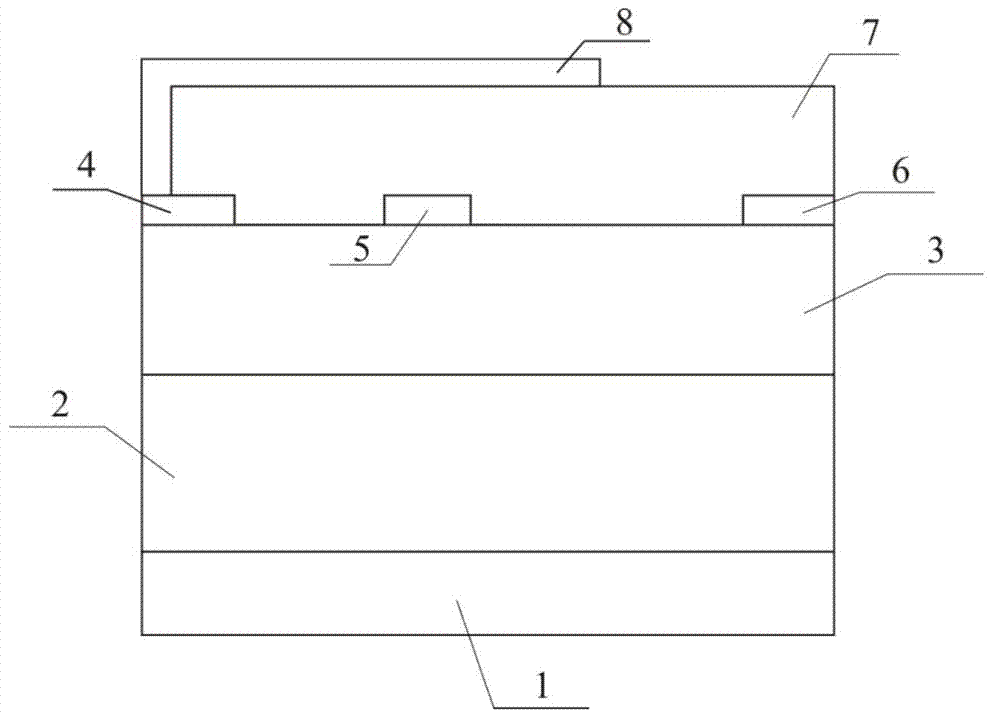
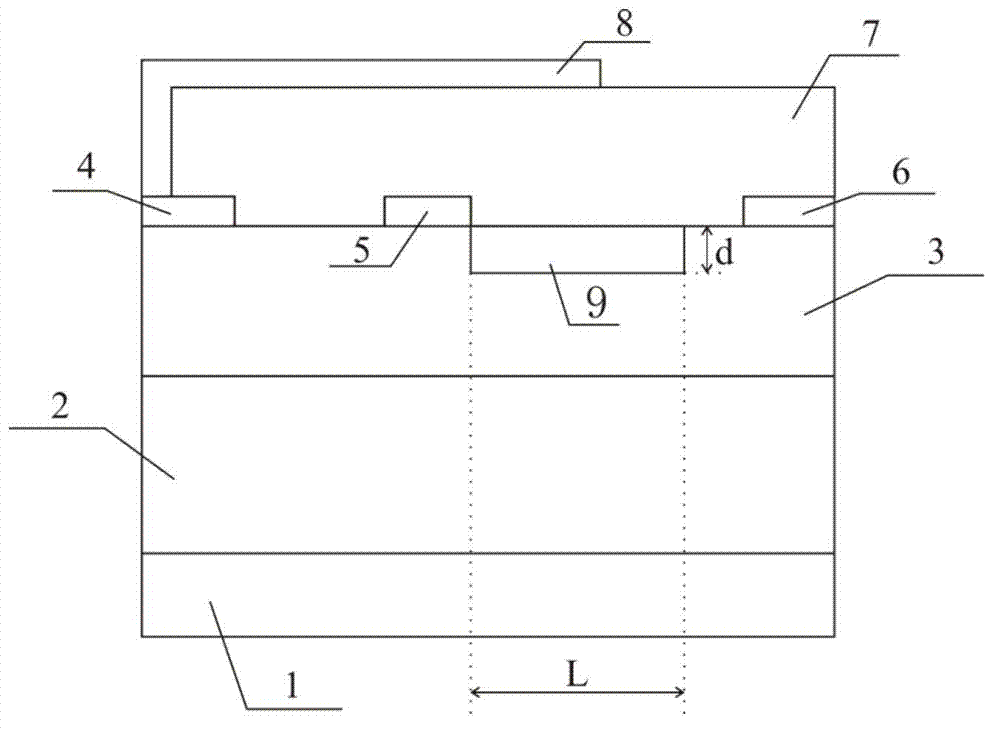
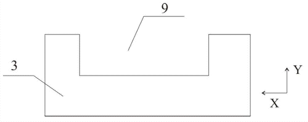
[0028] refer to figure 2 As shown, the gate edge groove type source field plate structure HEMT is based on the III-V compound semiconductor heterojunction structure, and its structure includes a substrate layer 1, a buffer layer 2, a barrier layer 3, and a source electrode 4 , gate 5, drain 6, passivation layer 7, source field plate 8 and gate edge groove 9 in the gate drain region; the buffer layer 2 is located on the substrate layer 1, and the barrier layer 3 is located in the buffer layer 2, the two ends of the upper part of the barrier layer 3 are the source 4 and the drain 6 respectively, and the middle is the gate 5; the passivation layer 7 is located on the source 4, the gate 5 and the drain 6, And on the barrier layer between the source and ...
PUM
 Abstract
Description
Claims
Application Information