Single-channel tunable filter in visible band based on one-dimensional photonic crystals
A dimensional photonic crystal and tuning filter technology, which is applied in the direction of optical waveguide light guide, light guide, optics, etc., can solve the problems of inability to achieve tuning and inability to tune the conduction band, and achieve the effects of easy acquisition, good filtering performance, and simple structure
- Summary
- Abstract
- Description
- Claims
- Application Information
AI Technical Summary
Problems solved by technology
Method used
Image
Examples
Embodiment 1
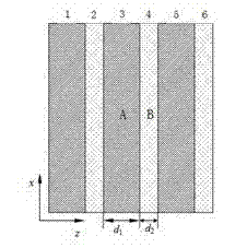
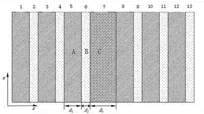
[0083] The two dielectric materials used in this example are lithium fluoride (dielectric constant 1.96) and gallium antimonide (dielectric constant 20.25), according to [LiF / GaSb] 3 The structural arrangement forms a one-dimensional photonic crystal. The thickness of lithium fluoride d 1 =0.78 ɑ =98.3nm, gallium antimonide thickness d 2 =0.22 ɑ =27.7nm, lattice constant ɑ =126.0nm.
[0084] A fully automatic magnetron sputtering coating machine model MSP-3200C is used to alternately grow lithium fluoride and gallium antimonide on the optical substrate by coating method, a total of 6 layers. First, the sixth layer of gallium antimonide is coated and grown on the optical substrate with a thickness of 27.7nm, and then the fifth layer of lithium fluoride is coated and grown on the sixth layer of gallium antimonide with a thickness of 98.3nm to obtain a period of the photonic crystal. Then use the same method to grow for 2 more cycles to obtain three cycles of [LiF / Ge] ...
Embodiment 2
[0088] The two dielectric materials used in this example are lithium fluoride (dielectric constant 1.96) and germanium (dielectric constant 16.00), according to [LiF / Ge] 3 The structural arrangement forms a one-dimensional photonic crystal. The thickness of lithium fluoride d 1 =0.74 ɑ =93.2nm, germanium thickness d 2 =0.26 ɑ =32.8m, lattice constant ɑ =126.0nm.
[0089] The preparation method of the one-dimensional photonic crystal single-channel tunable filter in the visible light band is the same as that in Example 1.
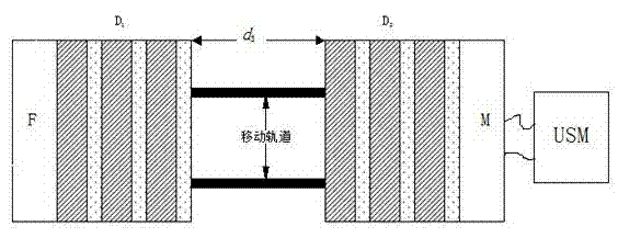
[0090] When the thickness of the air layer C d 3 at 0.3 a ~1.5 a When changing within the range, the transmittance characteristics of the tunable filter are as follows Figure 11 ~ Figure 17 As shown, the bandgap width increases with d 3 Widen with the increase of , always covering the entire visible light range, the position of the channel moves continuously between 418.3nm and 591.0nm, and the width changes between 1.3nm and 2.2nm.
Embodiment 3
[0092] The two dielectric materials used in this example are magnesium fluoride (dielectric constant 1.38) and germanium (dielectric constant 16.00), according to [MgF 2 / Ge] 3 The structural arrangement forms a one-dimensional photonic crystal. The thickness of lithium fluoride d 1 =0.76 ɑ =95.8nm, germanium thickness d 2 =0.24 ɑ =30.2nm, lattice constant ɑ =126.0nm.
[0093] The preparation method of the one-dimensional photonic crystal single-channel tunable filter in the visible light band is the same as that in Example 1.
[0094] When the thickness of the air layer C d 3 at 0.3 a ~1.5 a When changing within the range, the transmittance characteristics of the tunable filter are as follows Figure 18 ~ Figure 24 As shown, the bandgap width increases with d 3 The channel becomes wider and wider as it increases, and always covers the entire visible light range. The position of the channel moves continuously between 407.0nm and 584.4nm, and the width varies ...
PUM
 Abstract
Description
Claims
Application Information


