Cover plate-free carbon nanotube device structure and manufacturing method thereof

A carbon nanotube and device structure technology, applied in the field of nanoelectronic devices and sensors, can solve problems such as limited application range, difficulty in batch production, and high difficulty in device production, so as to simplify the process flow, improve device yield, device structure and The effect of simple manufacturing process

Active Publication Date: 2012-11-21
SHANGHAI INST OF MICROSYSTEM & INFORMATION TECH CHINESE ACAD OF SCI
View PDF5 Cites 2 Cited by
  • Summary
  • Abstract
  • Description
  • Claims
  • Application Information

AI Technical Summary

Problems solved by technology

In terms of infrared detection, in 2001, Xu Jianmin and others grew a multi-walled carbon nanotube array perpendicular to the substrate on a porous alumina template, and realized the detection of infrared light, but the device manufacturing process is complicated and the controllability is poor.
In 2006, MikhailE.Itkis and others used single-walled carbon nanotube films as sensitive elements to realize infrared detection, but the device is large in size and difficult to mass-produce, which limits the scope of application
In 2007, Jiangbo Zhang et al placed a single multi-walled carbon tube between the gold electrodes by means of AFM control, and made a single multi-walled carbon tube infrared sensitive device, but the device is difficult to manufacture and it is difficult to mass-produce
In terms of THz detection, in 2008, K.Fu et al. deposited single-walled carbon tubes on gold electrodes by electrophoresis, but this structure is difficult to achieve ohmic contact between electrodes and carbon tubes, and the signal-to-noise ratio of device detection is not high.

Method used


Image

  • Cover plate-free carbon nanotube device structure and manufacturing method thereof
  • Cover plate-free carbon nanotube device structure and manufacturing method thereof
  • Cover plate-free carbon nanotube device structure and manufacturing method thereof

Examples


Embodiment Construction

[0030] The specific implementation steps of the present invention will be further described below in conjunction with the accompanying drawings, which are not drawn to scale for the convenience of illustration.

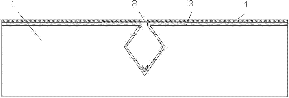
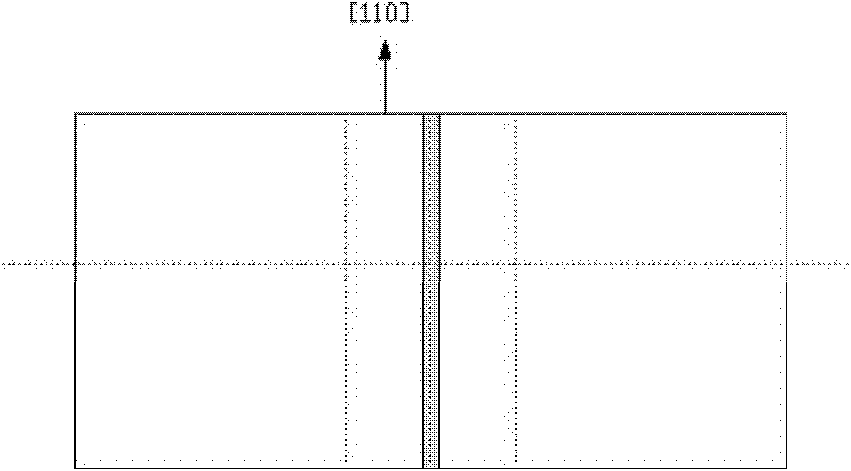
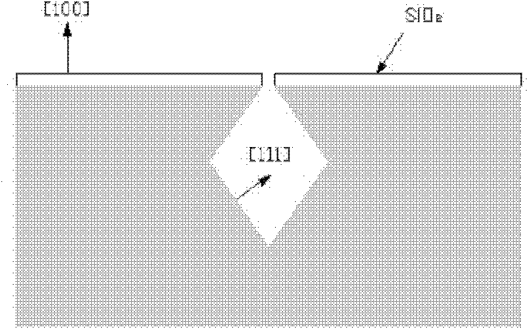
[0031] This embodiment provides a carbon nanotube sensor structure, which can be combined with MEMS technology as a carbon nanotube infrared and THz detector structure. The device structure is fabricated on a single crystal silicon substrate with a orientation, and the structure is as follows figure 1 As shown, it includes (100) single crystal silicon substrate 1 , horizontal single-walled carbon nanotube array 2 , oxide layer 3 , and metal electrode 4 in four parts. Wherein, the near-rhombic section groove in the (100) single crystal silicon substrate 1 is obtained by anisotropic wet etching on the basis of dry etching the deep groove. The opening of the groove is along the crystal direction, and the surface after wet etching is the (111) surface, such as Figure...


PUM

PropertyMeasurementUnit
widthaaaaaaaaaa
depthaaaaaaaaaa
thicknessaaaaaaaaaa

Abstract

The invention discloses a cover plate-free carbon nanotube device structure and a manufacturing method thereof. The structure includes a (100) monocrystalline silicon substrate, carbon nanotubes and a metal electrode. On the (100) monocrystalline silicon substrate is arranged a groove with a substantially rhombic section and running over the whole (100) monocrystalline silicon substrate width. The carbon nanotubes cross over the groove and keep suspended over the groove. The metal electrode is located on two sides of the groove and separately covers the parts of the carbon nanotubes crossing on the two sides of the groove, so that the carbon nanotubes and the metal electrode on the two sides of the groove form electrical connection. The inventive device structure is used for carbon nanotube electronic devices and sensors. As a cover plate is obviated, the device structure manufacturing process is simple and the yield is high so that the device structure is suitable for array production.

Description

technical field [0001] The invention relates to a carbon nanotube device structure and a manufacturing method thereof, in particular to a carbon nanotube device structure without a cover plate and a manufacturing method thereof, and is especially suitable for manufacturing large-scale carbon nanotube electronic devices and sensors. The invention belongs to the field of nanometer electronic devices and sensors. Background technique [0002] Carbon nanotubes are emerging functional nanomaterials. The detector made by it has the advantages of small size, low power consumption and high sensitivity. In terms of infrared detection, in 2001, Xu Jianmin and others grew multi-walled carbon nanotube arrays perpendicular to the substrate on a porous alumina template, realizing the detection of infrared light, but the device manufacturing process is complicated and the controllability is poor. In 2006, MikhailE.Itkis and others used single-walled carbon nanotube film as a sensitive el...

Claims


Application Information

Patent Timeline
Patent Type & Authority Applications(China)
IPC IPC(8): B81B1/00B81B7/04B81C1/00
Inventor 李铁周玉修王跃林
Owner SHANGHAI INST OF MICROSYSTEM & INFORMATION TECH CHINESE ACAD OF SCI
Why Eureka
Try Eureka