Tri-strain BiCMOS (Bipolar Complementary Metal Oxide Semiconductor) integrated device based on SiGe HBT (Heterojunction Bipolar Transistor) and preparation method

An integrated device, three-strain technology, applied in semiconductor/solid-state device manufacturing, electric solid-state devices, semiconductor devices, etc., can solve the problems of limitation, low mobility of Si material carrier materials, etc.

Inactive Publication Date: 2012-11-21
XIDIAN UNIV
View PDF2 Cites 6 Cited by
  • Summary
  • Abstract
  • Description
  • Claims
  • Application Information

AI Technical Summary

Problems solved by technology

[0007] Due to the low mobility of Si materials, the performance of integrated circuits manufactured by Si BiCMOS technology, especially the frequency performance, is greatly limited; for SiGe BiCMOS technology, although SiGe HBT is used for bipolar

Method used


Image

  • Tri-strain BiCMOS (Bipolar Complementary Metal Oxide Semiconductor) integrated device based on SiGe HBT (Heterojunction Bipolar Transistor) and preparation method

Examples


Embodiment 1

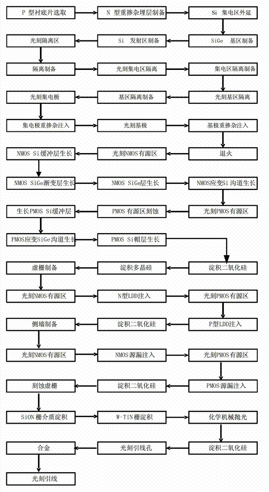
[0117] Embodiment 1: The three-strain BiCMOS integrated device and circuit based on SiGe HBT with a conductive channel of 45nm are prepared, and the specific steps are as follows:

[0118] Step 1, epitaxial growth.

[0119] (1a) Select the doping concentration to be 5×10 14 cm -3 A P-type Si sheet as a substrate;

[0120] (1b) Thermally oxidize a layer of SiO with a thickness of 300nm on the substrate surface 2 layer;

[0121] (1c) Photolithography of the buried layer region, implanting N-type impurities into the buried layer region, and annealing at 800°C for 90 minutes to activate the impurities to form an N-type heavily doped buried layer region;

[0122] (1d) Using chemical vapor deposition (CVD), grow a layer of N-type epitaxial Si layer with a thickness of 2 μm on the upper layer of Si material at 600 ° C, as the collector region, and the doping concentration of this layer is 1× 10 16 cm -3 ;

[0123] (1e) Using chemical vapor deposition (CVD), grow a layer of S...

Embodiment 2

[0183] Embodiment 2: The preparation of a three-strain BiCMOS integrated device and circuit based on SiGe HBT with a conductive channel of 30nm, the specific steps are as follows:

[0184] Step 1, epitaxial growth.

[0185] (1a) Select the doping concentration as 1×10 15 cm -3 A P-type Si sheet as a substrate;

[0186] (1b) Thermally oxidize a layer of SiO with a thickness of 400nm on the substrate surface 2 layer;

[0187] (1c) Photoetching the buried layer region, implanting N-type impurities into the buried layer region, and annealing at 900°C for 60 minutes to activate the impurities to form an N-type heavily doped buried layer region;

[0188] (1d) Using chemical vapor deposition (CVD), grow a layer of N-type epitaxial Si layer with a thickness of 2.5 μm on the upper layer of Si material at 700 ° C, as the collector region, and the doping concentration of this layer is 5 ×10 16 cm -3 ;

[0189] (1e) Using chemical vapor deposition (CVD), grow a layer of SiGe laye...

Embodiment 3

[0249] Embodiment 3: The preparation of a SiGe HBT-based three-strain BiCMOS integrated device and circuit with a 22nm conductive channel, the specific steps are as follows:

[0250] Step 1, epitaxial growth.

[0251] (1a) Select the doping concentration to be 5×10 15 cm -3 A P-type Si sheet as a substrate;

[0252] (1b) Thermally oxidize a layer of SiO with a thickness of 500nm on the surface of the substrate 2 layer;

[0253] (1c) Photolithography of the buried layer region, implanting N-type impurities into the buried layer region, and annealing at 950°C for 30 minutes to activate the impurities to form an N-type heavily doped buried layer region;

[0254] (1d) Using chemical vapor deposition (CVD), grow a layer of N-type epitaxial Si layer with a thickness of 3 μm on the upper layer of Si material at 750 ° C, as the collector region, and the doping concentration of this layer is 1× 10 17 cm -3 ;

[0255] (1e) Using chemical vapor deposition (CVD), grow a layer of ...


PUM

PropertyMeasurementUnit
Thicknessaaaaaaaaaa
Thicknessaaaaaaaaaa
Thicknessaaaaaaaaaa

Abstract

The invention discloses a tri-strain BiCMOS (Bipolar Complementary Metal Oxide Semiconductor) integrated device based on SiGe HBT (Heterojunction Bipolar Transistor) and a preparation method. A buried layer is prepared on a substrate, an N-Si layer, a P-SiGe layer and an N-Si layer are continuously grown, a dielectric layer is deposited, deep-groove isolation is prepared, a collector region, a base region and an emitter region are prepared, a collector electrode, base electrode and emitter electrode contact region is formed, and a SiGe HBT device is formed; active region deep grooves of an NMOS (N-channel Metal Oxide Semiconductor) device and a PMOS (P-channel Metal Oxide Semiconductor) device are etched, a P-type Si layer/a P-type SiGe gradient layer/a P-type SiGe layer/a P-type strain Si layer serving as the active region of the NMOS device and an N-type Si layer/an N-type strain SiGe layer/an N-type Si cap layer serving as the active region of the PMOS device are respectively and selectively grown in the deep grooves in an extending manner; a virtual grid electrode and a side wall are prepared, and source and drain electrodes of the NMOS and the PMOS device are formed through self-alignment; and the virtual grid is etched, a SiON grid dielectric layer and a W-TiN composite grid are deposited to form a CMOS structure, and finally the tri-stain BiCMOS integrated device and a circuit are constructed. Tensile strain Si with high electronic mobility and compressive strain SiGe with high hole mobility are sufficiently utilized as conducting channels for the NMOS device and the PMOS device, and the performance of the BiCMOS integrated circuit is effectively improved.

Description

technical field [0001] The invention belongs to the technical field of semiconductor integrated circuits, and in particular relates to a SiGe HBT-based three-strain BiCMOS integrated device and a preparation method. Background technique [0002] The integrated circuit, which appeared in 1958, is one of the most influential inventions of the 20th century. Microelectronics, which was born based on this invention, has become the basis of existing modern technology, accelerating the process of knowledge and informationization of human society, and at the same time changing the way of thinking of human beings. It not only provides humans with a powerful tool to transform nature, but also opens up a broad space for development. [0003] Semiconductor integrated circuits have become the basis of the electronics industry, and people's huge demand for the electronics industry has prompted the rapid development of this field. In the past few decades, the rapid development of the ele...

Claims


Application Information

Patent Timeline
IPC IPC(8): H01L27/06H01L21/8249
Inventor 胡辉勇宋建军宣荣喜周春宇张鹤鸣李妤晨舒斌郝跃
Owner XIDIAN UNIV
Why Eureka
Try Eureka