Double poly-crystal SOI (Silicon On Insulator) BiCMOS integrated device based on crystal plane selection and preparation method

An integrated device, dual polycrystalline technology, applied in semiconductor/solid-state device manufacturing, electric solid-state devices, semiconductor devices, etc., can solve the problems of limitation, low mobility of Si material carrier materials, etc.

Inactive Publication Date: 2012-12-12
XIDIAN UNIV
View PDF2 Cites 0 Cited by
  • Summary
  • Abstract
  • Description
  • Claims
  • Application Information

AI Technical Summary

Problems solved by technology

[0008] Due to the low mobility of Si material carrier materials, the performance of integrated circuits manufactured using Si BiCMOS technology, especially the frequency performance, is greatly limited; for SiGe BiCMOS technology, although SiGe HBT is used for bipolar transistors, However, Si CMOS is still used for unipolar devices that restrict the improvement of the frequency characteristics of BiCMOS integrated circuits, so these limit the further improvement of the performance of BiCMOS integrated circuits

Method used


Image

  • Double poly-crystal SOI (Silicon On Insulator) BiCMOS integrated device based on crystal plane selection and preparation method

Examples


Embodiment 1

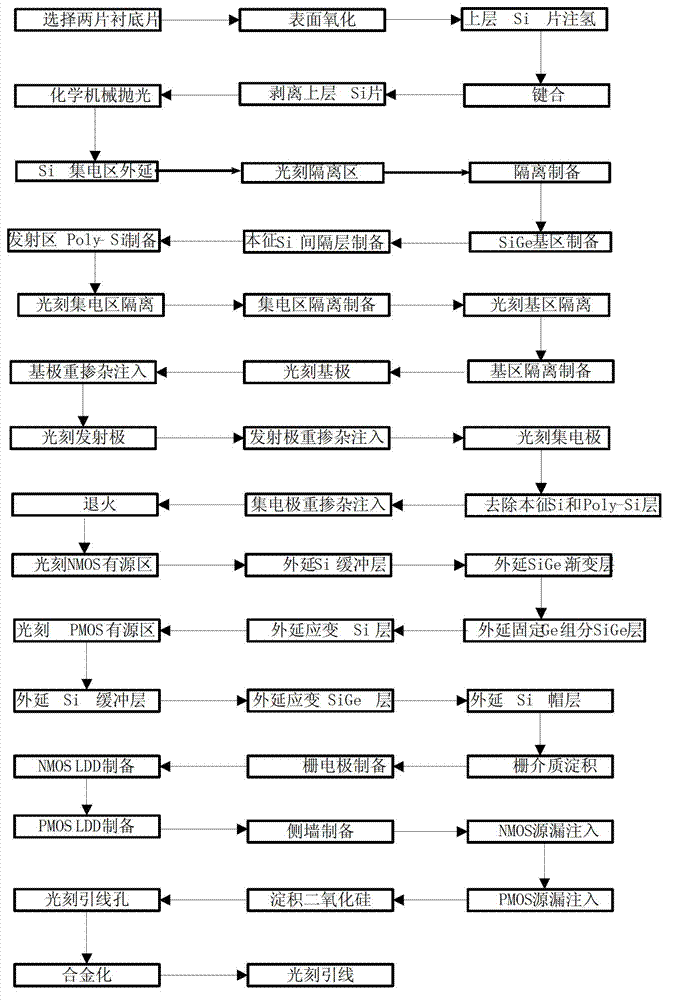
[0122] Embodiment 1: Prepare 22nm double-polycrystalline SOI BiCMOS integrated device and circuit based on crystal face selection, the specific steps are as follows:

[0123] Step 1, SOI substrate material preparation.

[0124] (1a) Select the N-type doping concentration as 1×10 15 cm -3 The Si wafer with a crystal plane of (110) is oxidized on the surface, and the thickness of the oxide layer is 0.5 μm, which is used as the base material of the upper layer, and hydrogen is injected into the base material;

[0125] (1b) Select the P-type doping concentration as 1×10 15 cm -3 The Si sheet with a crystal plane of (100) is oxidized on the surface, and the thickness of the oxide layer is 0.5 μm, which is used as the base material of the lower layer;

[0126] (1c) Using a chemical mechanical polishing (CMP) process to polish the surface of the lower layer and the upper layer of substrate material after hydrogen injection;

[0127] (1d) SiO on the surface of the lower and upper...

Embodiment 2

[0189] Embodiment 2: Preparation of 30nm double-polycrystalline SOI BiCMOS integrated device and circuit based on crystal plane selection, the specific steps are as follows:

[0190] Step 1, SOI substrate material preparation.

[0191] (1a) Select the N-type doping concentration as 3×10 15 cm -3 The Si wafer with a crystal plane of (110) is oxidized on the surface, and the thickness of the oxide layer is 0.75 μm, which is used as the base material of the upper layer, and hydrogen is injected into the base material;

[0192] (1b) Select the P-type doping concentration as 3×10 15 cm -3 The Si sheet with a crystal plane of (100) is oxidized on the surface, and the thickness of the oxide layer is 0.75 μm, which is used as the base material of the lower layer;

[0193] (1c) Using a chemical mechanical polishing (CMP) process to polish the surface of the substrate material of the lower layer and the upper layer of the active layer after injecting hydrogen, respectively;

[0194...

Embodiment 3

[0256] Embodiment 3: Preparation of 45nm double-polycrystalline SOI BiCMOS integrated device and circuit based on crystal plane selection, the specific steps are as follows:

[0257] Step 1, SOI substrate material preparation.

[0258] (1a) Select the N-type doping concentration as 5×10 15 cm -3 The Si sheet with a crystal plane of (110) is oxidized on the surface, and the thickness of the oxide layer is 1 μm, which is used as the base material of the upper layer, and hydrogen is injected into the base material;

[0259] (1b) Select the P-type doping concentration as 5×10 15 cm -3 The Si wafer with a crystal plane of (100) is oxidized on the surface, and the thickness of the oxide layer is 1 μm, which is used as the base material of the lower layer;

[0260] (1c) Using a chemical mechanical polishing (CMP) process to polish the lower layer and the surface of the upper substrate material after hydrogen injection;

[0261] (1d) SiO on the surface of the lower and upper subs...


PUM


Abstract

The invention discloses a double poly-crystal SOI (Silicon On Insulator) BiCMOS integrated device based on crystal plane selection and a preparation method. The preparation method comprises the following steps: preparing a SOI substrate; growing N-Si as a collector region of a bipolar device; photo-etching a base region; growing P-SiGe, i-Si and i-Poly-Si on the area of the base region, thereby forming an emitter, a base and a collector, and forming a SiGe HBT (Heterojunction Bipolar Transistor) device; etching a deep slot on an NMOS (N-channel Metal Oxide Semiconductor) device region, selectively growing a strain Si epitaxial layer and preparing an NMOS device; selectively growing a strain SiGe epitaxial layer on a PMOS (P-channel Metal Oxide Semiconductor) device active region, thereby preparing a PMOS device; and preparing a SOI BiCMOS integrated device and a circuit. According to the preparation method, a SOI BiCMOS integrated circuit with an enhanced property is prepared on the basis of the SOI substrate by fully utilizing the characteristics that the electronic mobility of a Si material is higher than that of a semiconductor Si material, the hole mobility of a compressive strain SiGe material is higher than that of the semiconductor Si material and the mobility ratio is anisotropic.

Description

technical field [0001] The invention belongs to the technical field of semiconductor integrated circuits, and in particular relates to a double-polycrystalline SOI BiCMOS integrated device based on crystal plane selection and a preparation method. Background technique [0002] In the contemporary era of highly developed information technology, microelectronic technology represented by integrated circuits is the key to information technology. As the fastest-growing, most influential and most widely used technology in human history, integrated circuits have become an important symbol to measure a country's scientific and technological level, comprehensive national strength and national defense strength. [0003] "Moore's Law", which has had a huge impact on the development of the microelectronics industry, states that the number of transistors on an integrated circuit chip doubles approximately every 18 months, and the performance also doubles. For more than 40 years, the wor...

Claims


Application Information

Patent Timeline
Patent Type & Authority Applications(China)
IPC IPC(8): H01L27/06H01L21/8249
Inventor 胡辉勇张鹤鸣周春宇宣荣喜宋建军吕懿舒斌郝跃
Owner XIDIAN UNIV
Why Eureka
Try Eureka