LED structure comprising quantum barriers with gradient potential barrier heights and method for manufacturing LED structure

A technology of LED structure and potential barrier height, applied in the field of optoelectronics, can solve the problems of limited efficiency improvement and no improvement in hole transport, and achieve the effects of improving distribution, enhancing internal quantum efficiency and light output power, and improving binding capacity.

Inactive Publication Date: 2015-02-18
JIANGSU YONGDING COMM
View PDF5 Cites 0 Cited by
  • Summary
  • Abstract
  • Description
  • Claims
  • Application Information

AI Technical Summary

Problems solved by technology

This document is aimed at the composition gradient of each quantum well in light-emitting diodes; the In composition gradient triangular quantum wells recorded in the literature, although the polarization effect of the GaN quantum barrier on the low In composition side of each well is very Weak, but there is still a high polarization effect with the GaN quantum barrier on the high In side of the well, so this structure can only partially increase the space coincidence rate of carriers, but has no effect on the transport of holes, so it has no effect on the transport of holes. The efficiency improvement of the whole device is very limited

Method used


Image

  • LED structure comprising quantum barriers with gradient potential barrier heights and method for manufacturing LED structure
  • LED structure comprising quantum barriers with gradient potential barrier heights and method for manufacturing LED structure
  • LED structure comprising quantum barriers with gradient potential barrier heights and method for manufacturing LED structure

Examples


Embodiment Construction

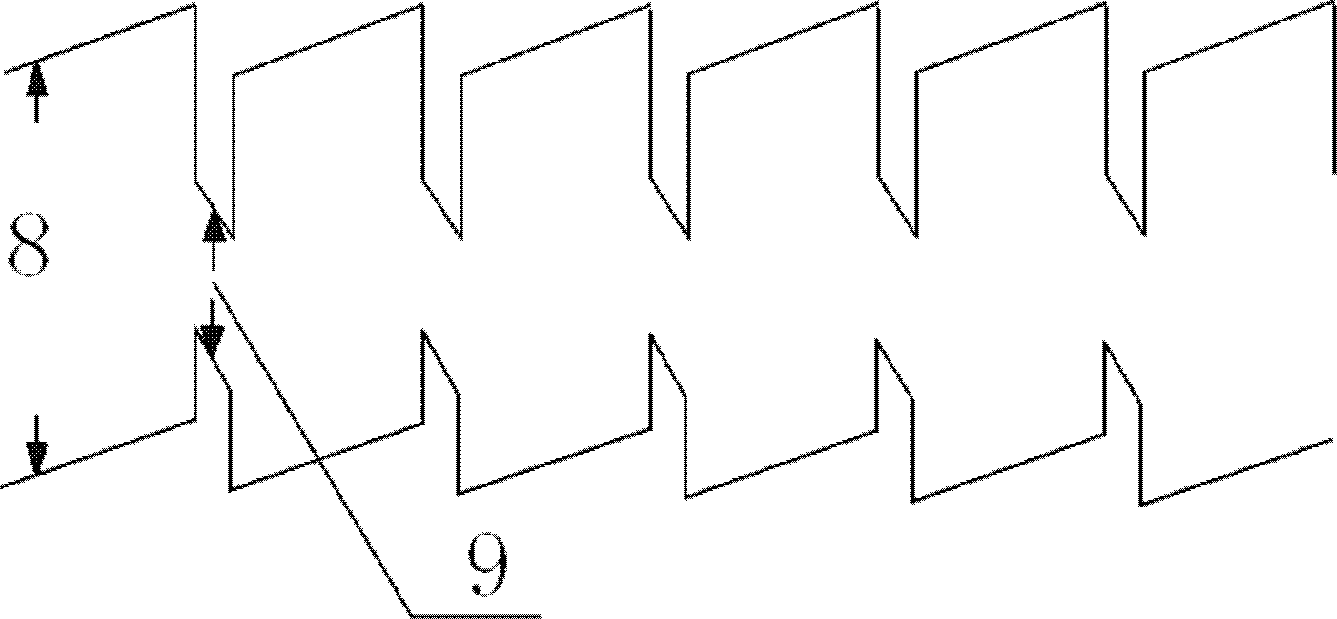
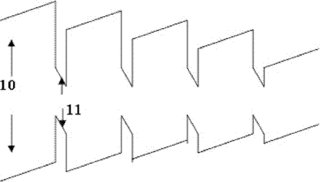
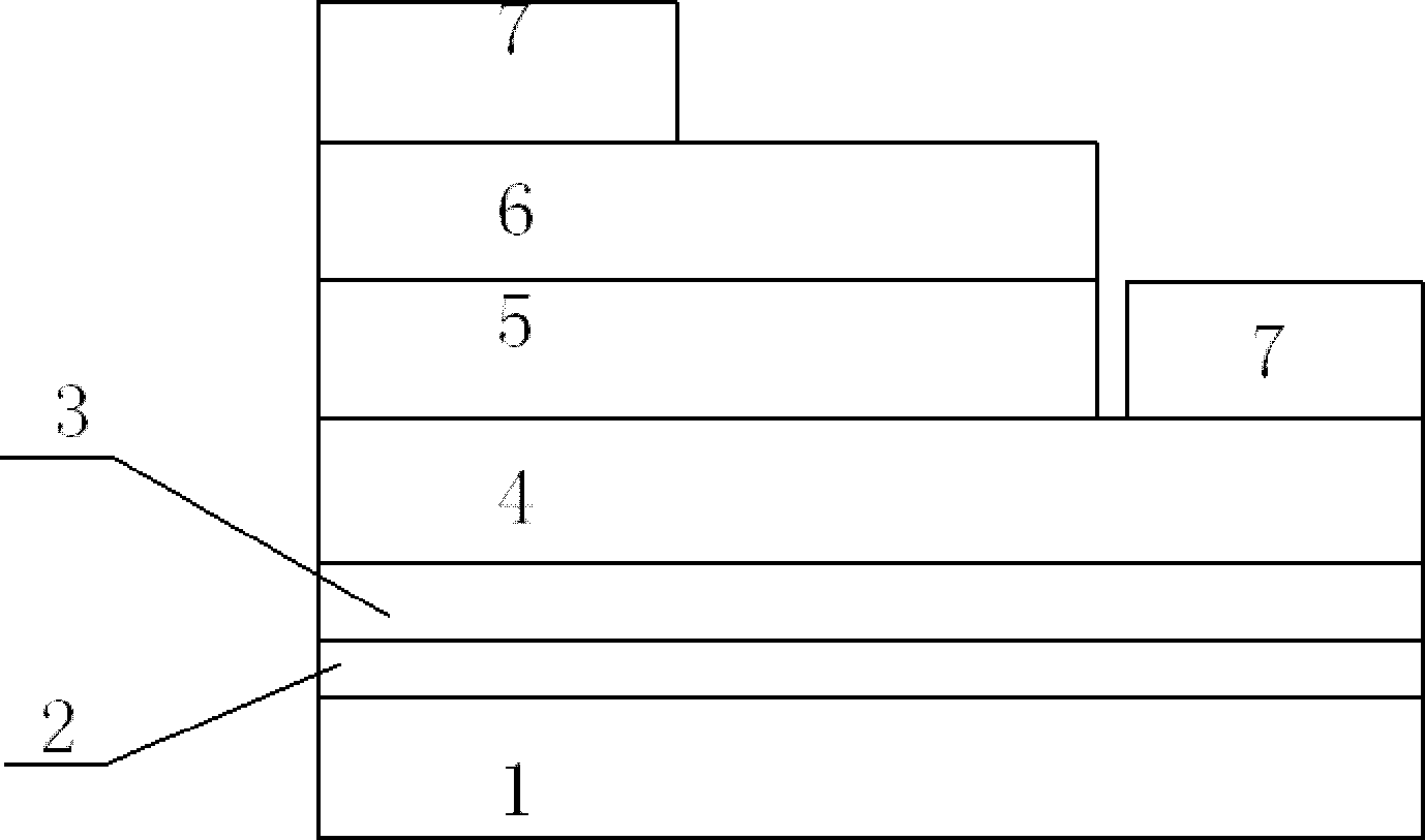
[0009] An LED structure using a quantum barrier with a gradient height of the potential barrier, including a nucleation layer, a buffer layer, an n-type conductive layer, a multi-quantum well layer and a p-type conductive layer on the substrate layer, and a p-type conductive layer on the n-type conductive layer. On the conductive layer are respectively ohmic contact layers; it is characterized in that, the described multi-quantum well layers are alternately grown Al with a thickness of 2-20nm x Ga 1-x-y In y N-well and Al with a thickness of 10-30nm u Ga 1-u-v In v N barriers, 2-30 repetition periods; among them, 0u Ga 1-u-v In v N, the value of u and v will meet the following conditions: make the potential barrier height of quantum barrier (that is, the forbidden band width) gradually reduce from the n side to the p side; and the forbidden band width of the quantum barrier is greater than the forbidden band width of the quantum well material . According to the general ...


PUM


Abstract

The invention relates to an LED structure comprising quantum barriers with gradient potential barrier heights and a method for manufacturing the LED structure, and belongs to the technical field of photoelectrons. The LED structure is provided with a plurality of quantum well layers, and the potential barrier heights of the quantum barriers are gradually reduced from an n side to a p side. Conveyance of electron holes is improved owing to the novel structure, so that the electron holes can be distributed in large quantities of quantum wells, and the intensity of polarization among the potential barriers is reduced in general. Owing to the factors, the distribution of the concentration of electrons and the distribution of the concentration of the electron holes are improved totally, the rate and the intensity of spontaneous radiation are increased totally, and accordingly, the internal quantum efficiency of a device is effectively enhanced, and outputted optical power of the device is effectively increased.

Description

technical field [0001] The invention relates to an LED structure adopting a gradient quantum barrier of potential barrier height and a preparation method thereof, belonging to the technical field of optoelectronics. Background technique [0002] III-V wide band gap direct band gap semiconductor has a series of advantages of wide band gap, high electron mobility, high thermal conductivity, high hardness, stable chemical properties, small dielectric constant and high temperature resistance, so its high brightness Blue light-emitting diodes, blue semiconductor lasers, and electronic power devices such as radiation-resistant, high-frequency, high-temperature, and high-voltage devices have a wide range of practical applications and huge market prospects. GaN is the basic material of semiconductor Group III nitrides. It has a hard texture and extremely stable chemical properties. It does not react with acids and alkalis at room temperature, is insoluble in water, and has a relativ...

Claims


Application Information

Patent Timeline
Patent Type & Authority Patents(China)
IPC IPC(8): H01L33/14H01L33/06H01L33/00
Inventor 王成新王强徐现刚李树强曲爽
Owner JIANGSU YONGDING COMM
Why Eureka
Try Eureka