Integrated manufacturing method of silicon base plate and copper micro heat pipe of LED (light emitting diode) apparatus
A technology for LED devices and manufacturing methods, applied in semiconductor devices, electrical components, circuits, etc., can solve problems such as copper layer thickness, and achieve the effects of small overall thermal resistance, improved reliability and life, and stable heat transfer
- Summary
- Abstract
- Description
- Claims
- Application Information
AI Technical Summary
Problems solved by technology
Method used
Image

Examples
Embodiment 1
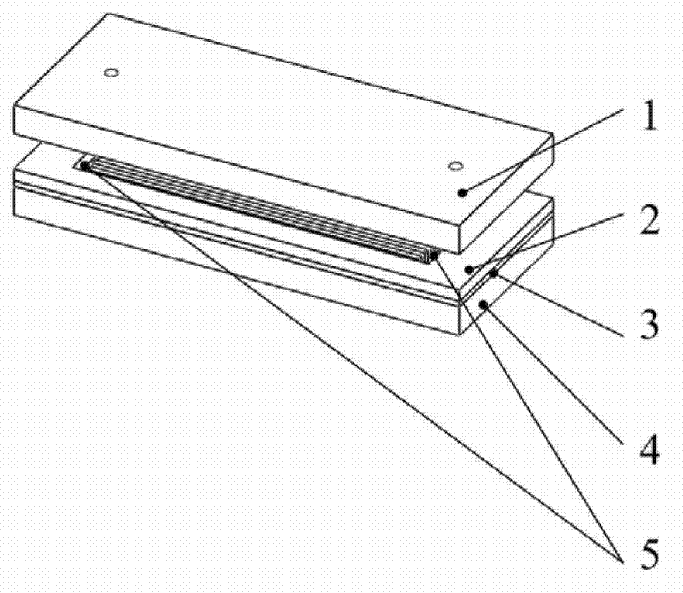
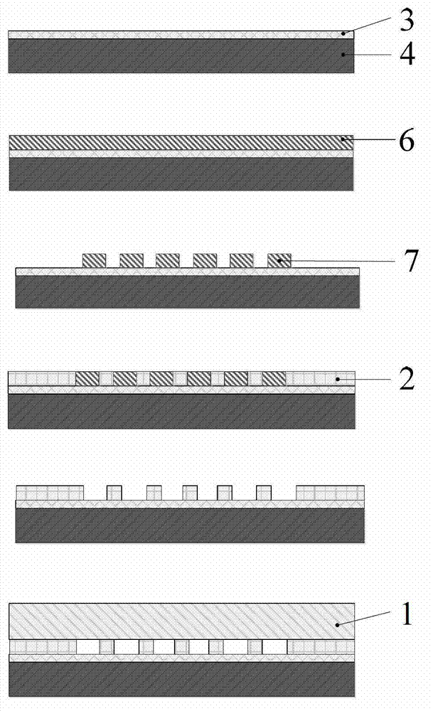
[0015] First, a copper seed layer 3 with a thickness of 150 nm is obtained on the back surface of the silicon substrate 4 by sputtering. Then, spin-coat SU-8 glue 6. When the model of SU-8 glue 6 is 2075, pre-coat with a glue homogenizer at a speed of 500rpm for 15s, and then spin-coat at a speed of 2000rpm for 45s to obtain a glue thickness of 100μm. Pre-bake the SU-8 glue at 85°C for 90 minutes, bake the SU-8 glue at 85°C for 5 minutes after photolithography on a photolithography machine, and then develop it to obtain the SU-8 glue electroforming mold 7.
[0016] In the electroforming machine, electroform copper on the SU-8 glue electroforming mold 6 until it is consistent with the thickness of the glue layer of the mold and stop, remove the SU-8 glue in the degumming solution of the SU-8 glue, and obtain Copper microstructure2. Cut a piece of pure copper plate 1 of the same size as the silicon substrate on a 0.5 mm thick pure copper plate, and use mechanical processing met...
Embodiment 2
[0018] First, a copper seed layer 3 with a thickness of 200 nm is obtained on the back surface of the silicon substrate 4 by sputtering. Then, spin coat SU-8 glue6. When the model of SU-8 glue 6 is 3100, pre-coat with a glue leveler at a speed of 500rpm for 15s, and then spin coat at a speed of 1000rpm for 45s to obtain a glue thickness of 250μm. Pre-bake the SU-8 glue at 85°C for 150 minutes, bake the SU-8 glue at 85°C for 15 minutes after photolithography on a photolithography machine, and then develop it to obtain the SU-8 glue electroforming mold 7.
[0019] In the electroforming machine, electroform copper on the SU-8 glue electroforming mold 6 until it is consistent with the thickness of the glue layer of the mold and stop, remove the SU-8 glue in the degumming solution of the SU-8 glue, and obtain Copper microstructure2. Cut a piece of pure copper plate 1 of the same size as the silicon substrate on a 0.5 mm thick pure copper plate, and use mechanical processing metho...
Embodiment 3
[0021] First, a copper seed layer 3 with a thickness of 200 nm is obtained on the back surface of the silicon substrate 4 by sputtering. Then, spin coat SU-8 glue6. When the model of SU-8 glue 6 is 3100, pre-coat at 500rpm for 15s, then spin coat at 800rpm for 45s to obtain a glue thickness of 300μm. Pre-bake the SU-8 glue at 85°C for 200 minutes, and after photolithography on the photolithography machine, bake the SU-8 glue at 85°C for 30 minutes before developing to obtain the SU-8 glue electroforming mold 7.
[0022] In the electroforming machine, electroform copper on the SU-8 glue electroforming mold 6 until it is consistent with the thickness of the glue layer of the mold and stop, remove the SU-8 glue in the degumming solution of the SU-8 glue, and obtain Copper microstructure2. Cut a piece of pure copper plate 1 of the same size as the silicon substrate on a 0.5 mm thick pure copper plate, and use mechanical processing methods, such as drilling, to obtain heat pipe w...
PUM
| Property | Measurement | Unit |
|---|---|---|
| Thickness | aaaaa | aaaaa |
| Thickness | aaaaa | aaaaa |
Abstract
Description
Claims
Application Information
 - Generate Ideas
- Intellectual Property
- Life Sciences
- Materials
- Tech Scout
- Unparalleled Data Quality
- Higher Quality Content
- 60% Fewer Hallucinations
Browse by: Latest US Patents, China's latest patents, Technical Efficacy Thesaurus, Application Domain, Technology Topic, Popular Technical Reports.
© 2025 PatSnap. All rights reserved.Legal|Privacy policy|Modern Slavery Act Transparency Statement|Sitemap|About US| Contact US: help@patsnap.com