
Method for preparing monocrystalline silicon carbide nano-wires on flexible carbon fiber substrate

A technology for silicon carbide nanowires and single crystal silicon carbide, applied in the field of preparing single crystal silicon carbide nanowires, can solve the problems of complex preparation method, low yield, poor orientation of silicon carbide nanowires, etc. high rate effect

Inactive Publication Date: 2012-12-19
PLA SECOND ARTILLERY ENGINEERING UNIVERSITY
View PDF9 Cites 12 Cited by
  • Summary
  • Abstract
  • Description
  • Claims
  • Application Information

AI Technical Summary

Problems solved by technology

In addition, these methods require special instruments and equipment, low yields, and complicated preparation methods to varying degrees.
The growth of silicon carbide nanowires has disadvantages such as poor orientation

Method used


Image

  • Method for preparing monocrystalline silicon carbide nano-wires on flexible carbon fiber substrate
  • Method for preparing monocrystalline silicon carbide nano-wires on flexible carbon fiber substrate

Examples


Embodiment

[0020] The whole silicon carbide nanowire growth process includes the following steps:

[0021] Step 1: Soak a commercially available carbon fiber cloth in 0.3 mol / l ferric nitrate solution for 1 hour, then take it out, and dry it in a drying box.

[0022] Step 2: Put 14 grams of silicon powder into the alumina crucible, then cover the weighed 6 grams of carbon fiber cloth, and press the top of the carbon fiber cloth with a cover;

[0023] Step 3: Put the whole reaction device into the tube furnace, evacuate to 0.1Pa, and then pass in argon protection;

[0024] Step 4: Heat to 1500°C, keep warm for 6 hours, and then cool naturally.

[0025] Step 5: Take out the reacted carbon fiber cloth directly. At this time, a large number of silicon carbide nanowire arrays are lined with the carbon fiber cloth.

[0026] see figure 1 : Schematic diagram of the device for growing silicon carbide nanowire arrays and reacting in a horizontal tube furnace

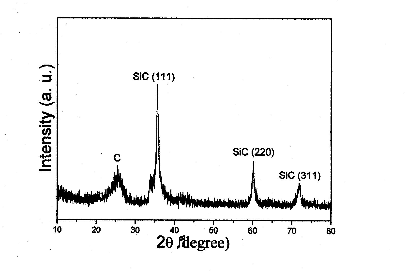
[0027] see figure 2 : The XRD p...


PUM

PropertyMeasurementUnit
diameteraaaaaaaaaa

Abstract

The invention relates to a method preparing monocrystalline silicon carbide nano-wires on a flexible carbon fiber substrate. A carbon fiber cloth in the market is soft and curving, can be a carbon source required by the growth of silicon carbide nano-wires, and also can be used as a flexible substrate to deposit a silicon carbide nano-wire array, so a massive-growth monocrystalline silicon carbide nano-wire array is prepared on the flexible substrate through utilizing the above superior characteristics of the carbon fiber cloth. The method is characterized in that the method has the advantages of easily available raw material, low cost and simple technology; argon protects as an inert gas, flows or does not flows, and has no special requirements on reaction equipment, so any high-temperature furnace capable of heating can be used; the flexible carbon fiber cloth is adopted as the substrate to deposit the silicon carbide nano-wires, is also adopted as the carbon source, participates in the above reaction, and maintains a certain flexible property after the reaction; the carbon fiber can also be adopted as the flexible substrate to prepare other carbide nano-materials; and the grown silicon carbide nano-wires have the advantages of certain orientation, good crystallinity, and high yield.

Description

technical field [0001] The invention belongs to the technical field of nanomaterial preparation and relates to a method for preparing single crystal silicon carbide nanowires on a flexible carbon fiber substrate. Background technique [0002] One-dimensional nanomaterials, such as nanowires, nanofibers, nanorods, nanobelts, etc., are widely used in nanoelectronic devices and nanolasers due to their unique electrical, optical, magnetic and other physical and chemical properties. , biosensors and nanocomposites. As an important semiconductor nanomaterial, silicon carbide nanowires have excellent characteristics such as wide band gap, high breakdown electric field strength, high thermal conductivity, and good chemical stability. These characteristics make silicon carbide nanowires play an important role in the construction of nano-optoelectronic devices. critical use. At present, there are many methods for preparing silicon carbide nanowires, which can be roughly divided into...

Claims


Application Information

Patent Timeline
Patent Type & Authority Applications(China)
IPC IPC(8): C30B29/36C30B29/62C30B25/00C30B25/18
Inventor 汪刘应吴仁兵刘顾
Owner PLA SECOND ARTILLERY ENGINEERING UNIVERSITY
Learn More