Mixed silicon single mode annular cavity laser based on microstructural silicon waveguide frequency selection

A microstructure, silicon waveguide technology, applied in the structure of the active area, the structure of the optical resonator, the structure of the optical waveguide semiconductor, etc., to achieve the effects of reducing reflected energy loss, high output optical power, and large side mode suppression ratio

Inactive Publication Date: 2014-01-01
INST OF SEMICONDUCTORS - CHINESE ACAD OF SCI
View PDF1 Cites 2 Cited by
  • Summary
  • Abstract
  • Description
  • Claims
  • Application Information

AI Technical Summary

Problems solved by technology

At present, there is no report on the realization of silicon-based hybrid single longitudinal mode laser through the dual function of microstructure and ring cavity

Method used


Image

  • Mixed silicon single mode annular cavity laser based on microstructural silicon waveguide frequency selection
  • Mixed silicon single mode annular cavity laser based on microstructural silicon waveguide frequency selection
  • Mixed silicon single mode annular cavity laser based on microstructural silicon waveguide frequency selection

Examples


Embodiment Construction

[0026] Silicon-based lasers are the core devices in photonic chips, and play an extremely important role in on-chip optical interconnection and optical switching.

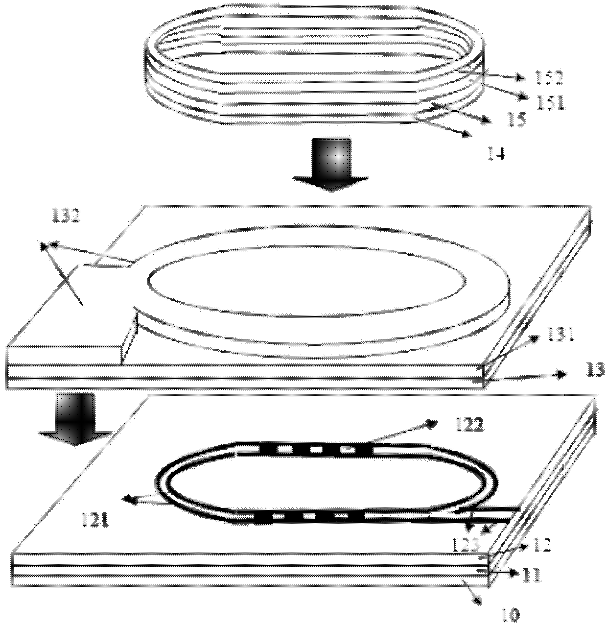
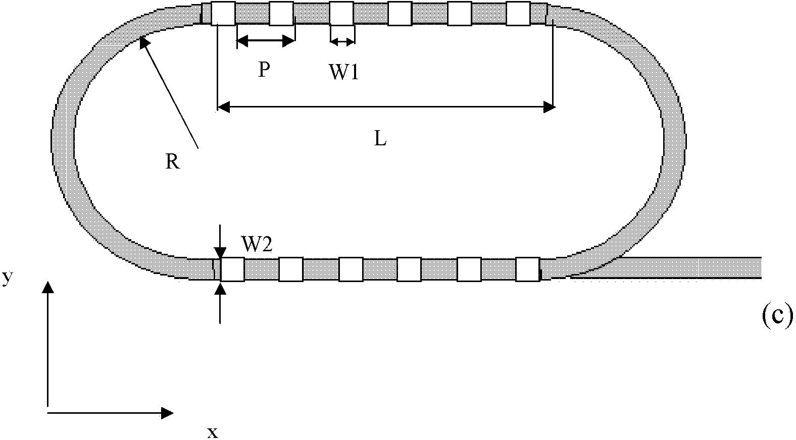
[0027] see figure 1 and figure 2 As shown, the present invention proposes a silicon-based integrated light source with single-mode operating characteristics, which uses a hybrid structure of silicon-based and III-V semiconductor materials. In the case of electrical injection, through evanescent field coupling and silicon-based The single-mode lasing is realized by the annular cavity and periodic microstructure on the surface, and the output light is coupled into the silicon-based waveguide. The gain medium adopts semiconductor multi-quantum well structure, and coplanar electrodes are used to realize electric injection. The III-V capping layer and active multi-quantum well also adopt annular cavity mode, and there can be microstructures on it. The laser is suitable for high-density photonic optoelectronic integra...


PUM


Abstract

The invention discloses a mixed silicon single mode annular cavity laser based on microstructural silicon waveguide frequency selection, comprising a silicon substrate, a silicon dioxide layer formed on the silicon substrate, a silicon annular waveguide layer formed on the silicon dioxide layer, a bonding buffer layer formed on the silicon waveguide layer, an N type contact layer formed on the bonding buffer layer, an N type electrode formed in the middle on the N type contact layer, an annular quantum well active region formed in an annular part of the N type electrode on the N type contact layer, a P type annular contact layer formed on the annular quantum well active region, a P type annular cover layer formed on the P type annular contact layer and a P type electrode formed on the P type annular cover layer. The structure is in high density integration, single longitudinal mode working and high-efficiency coupling outputting; and more importantly, according to the mixed silicon single mode annular cavity laser disclosed by the invention, technological steps of conventional DFB distributed feedback grating manufacturing, III-V group material secondary epitaxy and the like are saved in technological processing, and the complexity is lowered.

Description

technical field [0001] The invention relates to the technical field of photonic optoelectronic device design, in particular to a mixed silicon-based single longitudinal mode ring cavity microstructure laser, which is suitable for photonic optoelectronic integration applications. Background technique [0002] Silicon-based semiconductors are the cornerstone of the modern microelectronics industry, but they are reaching their limits, especially when it comes to interconnects. However, optoelectronic technology is in a stage of rapid development. Today's semiconductor light-emitting devices are mostly made of compound materials, which are not compatible with silicon microelectronics technology. Therefore, it is meaningful to integrate photonic technology and microelectronic technology to develop silicon-based optoelectronics science and technology. major. [0003] The hybrid laser of indium phosphide and silicon is considered to be the most promising technology suitable for hi...

Claims


Application Information

Patent Timeline
Patent Type & Authority Patents(China)
IPC IPC(8): H01S5/10H01S5/30H01S5/22
Inventor 张冶金王海玲渠红伟马绍栋郑婉华
Owner INST OF SEMICONDUCTORS - CHINESE ACAD OF SCI
Why Eureka
Try Eureka