Novel focal plane array electrical interconnection process

A focal plane array and electrical interconnection technology, applied in circuits, electrical components, electrical solid devices, etc., can solve problems such as increased thermal conductivity and deformation of indium columns, and achieve the effects of improving performance and avoiding increased thermal conductivity

Inactive Publication Date: 2013-01-16
CHANGCHUN INST OF OPTICS FINE MECHANICS & PHYSICS CHINESE ACAD OF SCI
View PDF5 Cites 23 Cited by
  • Summary
  • Abstract
  • Description
  • Claims
  • Application Information

AI Technical Summary

Problems solved by technology

[0007] In order to solve the problem of increased thermal conductance caused by the deformation of the indium column during the cold pressure welding process of the focal plane d

Method used


Image

  • Novel focal plane array electrical interconnection process
  • Novel focal plane array electrical interconnection process

Examples


Embodiment Construction

[0020] The present invention will be described in further detail below in conjunction with the accompanying drawings.

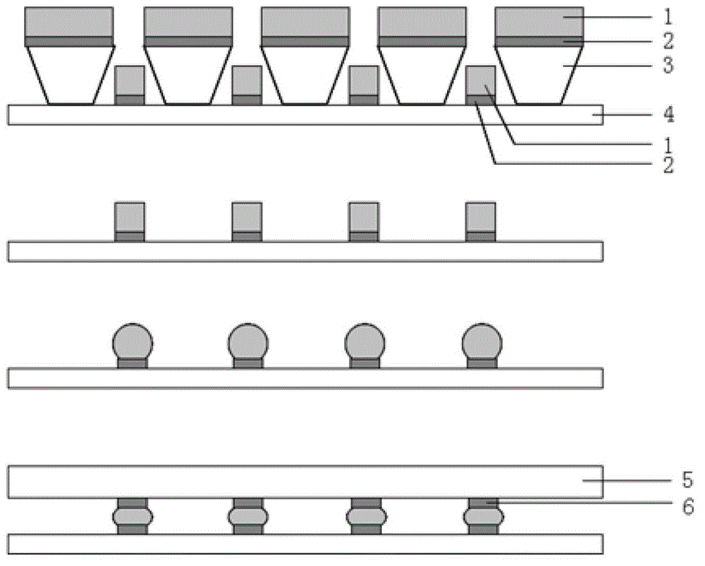
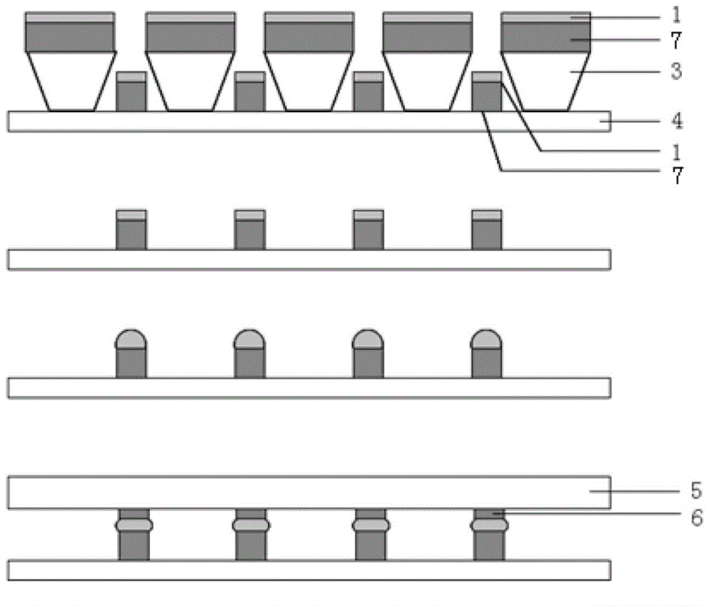
[0021] Such as figure 2 As shown, the present invention is a novel focal plane array electrical interconnection process.

[0022] First, the photolithography process on the readout circuit is carried out. This process is exposed through an ultraviolet mask to form a pattern on the photoresist 3 . The thickness of the photoresist 3 should be greater than or equal to the thickness of the deposited metal film, and the inclination angle between the side wall of the pattern and the surface of the readout circuit 4 should be less than or equal to 90°, that is, the pattern is an inverted trapezoid or rectangle, so as to facilitate the formation of the photoresist after coating. 3 strips.

[0023] Next is the deposition of the metal film. There are many methods that can be used in this process, such as electron beam evaporation, magnetron sputtering and so on. He...


PUM


Abstract

The invention belongs to the technical field of photoelectronic imaging and relates to a novel focal plane array electrical interconnection process which solves the problem of increase of thermal conductance caused by deformation of indium columns during cold welding of a focal plane detector. The focal plane array electrical interconnection process includes the steps: firstly, a photoetching process on a read-out circuit of the focal plane detector; secondly, a metal membrane deposition process, namely depositing a nickel or copper metal membrane and then depositing an indium metal membrane, wherein the nickel or copper metal membrane is thicker than the indium metal membrane; thirdly, a photoresist stripping process on the read-out circuit; fourthly, an indium column reflux balling process on the read-out circuit; fifthly, an electrode manufacturing process on a focal plane chip; and sixthly, a cold welding interconnection process of the focal plane chip and the read-out circuit. Since nickel or copper is used as indium column support and electrical communication metal, the problem of increase of thermal conductance caused by deformation of indium columns during cold welding interconnection is avoided, and performances of the focal plane array detector are improved.

Description

technical field [0001] The invention relates to a novel focal plane array electrical interconnection process, which belongs to the technical field of photoelectric imaging. Background technique [0002] Focal plane arrays are widely used in the research and development of various optoelectronic devices, such as focal plane infrared detectors, ultraviolet detectors and so on. Taking the focal plane infrared detector as an example, it is an infrared detector that works at room temperature, uses the pyroelectric effect to convert long-wave infrared radiation into electrical signals, and realizes scanning thermal imaging. The device is mainly composed of an infrared focal plane detector chip and a flip-chip interconnection of a readout circuit. It is characterized in that the detector chip and the readout circuit chip are prepared separately to optimize their respective performances and then interconnected. The interconnection between the detector chip and the readout circuit ...

Claims


Application Information

Patent Timeline
IPC IPC(8): H01L21/603H01L21/768
CPCH01L2224/11
Inventor 王泰升鱼卫星卢振武孙强
Owner CHANGCHUN INST OF OPTICS FINE MECHANICS & PHYSICS CHINESE ACAD OF SCI
Why Eureka
Try Eureka