Amorphous tellurium-cadmium-mercury/crystalline silicon heterojunction infrared-detector and manufacturing method thereof

An infrared detector, silicon heterojunction technology, applied in final product manufacturing, sustainable manufacturing/processing, semiconductor devices, etc. Reduced weight and good lattice matching performance

Inactive Publication Date: 2013-01-30
KUNMING INST OF PHYSICS
View PDF3 Cites 6 Cited by
  • Summary
  • Abstract
  • Description
  • Claims
  • Application Information

AI Technical Summary

Problems solved by technology

There is no research report on amorphous mercury cadmium telluride / crystalline silicon (a-HgCdTe / c-Si) heterojunction infrared detectors

Method used


Image

  • Amorphous tellurium-cadmium-mercury/crystalline silicon heterojunction infrared-detector and manufacturing method thereof
  • Amorphous tellurium-cadmium-mercury/crystalline silicon heterojunction infrared-detector and manufacturing method thereof
  • Amorphous tellurium-cadmium-mercury/crystalline silicon heterojunction infrared-detector and manufacturing method thereof

Examples


Embodiment 1

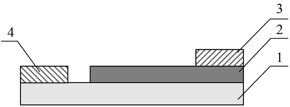
[0031] as attached figure 1 As shown, this figure is an embodiment of the a-HgCdTe / c-Si heterojunction infrared detector described in the present invention. It consists of c-Si substrate 1, a-HgCdTe thin film 2, Cr / Au alloy metal first electrode 3 and Cr / Au alloy metal second electrode 4, wherein the c-Si substrate is n-type crystalline semiconductor material , the c-Si substrate is not only used as the substrate, but also one of the materials that constitute the heterojunction; the a-HgCdTe film is an amorphous semiconductor material that is not intentionally doped, and its thickness is 1-2 μm; the heterojunction consists of a- Composed of HgCdTe film and c-Si substrate, a-HgCdTe film and c-Si substrate have good lattice matching, a-HgCdTe film and c-Si substrate are directly connected; metal first electrode and a-HgCdTe film connected, the metal second electrode is connected to the c-Si substrate.

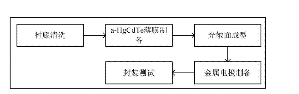
[0032] The preparation process of the a-HgCdTe / c-Si heterojunction infrare...

Embodiment 2

[0041] attached Figure 5What is shown is another embodiment of the a-HgCdTe / c-Si heterojunction infrared detector described in the present invention. The technical feature of this embodiment is that: the metal first electrode 3 and the metal second electrode 4 are ring-shaped electrode structures; The -Si substrate is directly connected, but the a-HgCdTe thin film 2 is not connected to the second metal electrode 4 and is separated; the first metal electrode 3 is located on the a-HgCdTe thin film 2 and is directly connected to it. The rest of the technical features are the same as those in Embodiment 1.

[0042] The preparation process of the a-HgCdTe / c-Si heterojunction infrared detector of the present embodiment is as follows (such as Figure 8 shown):

[0043] The first step, substrate cleaning: the same as Step 1 in Embodiment 1;

[0044] The second step, preparation of the second metal electrode: preparing a ring-shaped second metal electrode 4 on the upper surface of...

Embodiment 3

[0051] attached Image 6 What is shown is another embodiment of the a-HgCdTe / c-Si heterojunction infrared detector described in the present invention. The technical feature of this embodiment is that the metal first electrode 3 is a circular electrode structure, and the metal second electrode 4 is a circular electrode structure; the c-Si substrate 1 is located on the metal second electrode 4 and is connected to it; a-HgCdTe The thin film 2 is located on the c-Si substrate and connected to it; the metal first electrode 3 is located on the a-HgCdTe thin film 2 and directly connected to it. The rest of the technical features are the same as those in Embodiment 1.

[0052] The preparation process of the a-HgCdTe / c-Si heterojunction infrared detector of the present embodiment is as follows (such as Figure 8 shown):

[0053] The first step, substrate cleaning: the same as Step 1 in Embodiment 1;

[0054] The second step, preparation of the second metal electrode: prepare a circ...


PUM

PropertyMeasurementUnit
thicknessaaaaaaaaaa
thicknessaaaaaaaaaa

Abstract

The invention relates to an amorphous tellurium-cadmium-mercury/crystalline silicon heterojunction infrared-detector, which is characterized by being composed of a crystalline silicon substrate, amorphous tellurium-cadmium-mercury, a first metal electrode and a second metal electrode, wherein the amorphous tellurium-cadmium-mercury and the crystalline silicon substrate form heterojunction, the first metal electrode is connected with the amorphous tellurium-cadmium-mercury, and the second metal electrode is connected with the crystalline silicon substrate. The preparation process comprises the following steps of substrate cleaning, amorphous tellurium-cadmium-mercury film preparation, photosensitive surface forming, metal electrode preparation and package test; or substrate cleaning, second metal electrode preparation, amorphous tellurium-cadmium-mercury film preparation, photosensitive surface forming, first metal electrode preparation and package test. The amorphous semiconductor material has no selectivity for the substrate, the lattice matching performance between materials forming heterojunction is better, and the significant photoelectric response exists. The optimum working temperature of the detector is close to room temperature, two stages of semiconductors are utilized for refrigeration, and the weight, the power consumption and the manufacturing cost of the infrared detector assembly are reduced.

Description

technical field [0001] The invention belongs to the technical field of heterojunction uncooled infrared detectors, in particular to a heterojunction infrared detector capable of working at room temperature based on amorphous semiconductor and crystalline semiconductor materials and a manufacturing method thereof. Background technique [0002] Crystalline mercury cadmium telluride (c-HgCdTe) thin films are the main infrared photodetector materials, and photovoltaic devices are often dominated by p-n junctions. Heterojunction detectors have the advantages of high sensitivity and fast response. In recent years, people have gradually focused their attention on the research of HgCdTe heterojunction infrared detectors. There are advantages of lattice matching, good uniformity and low cost between the silicon substrate and the Si readout circuit, so the silicon-based HgCdTe focal plane detector has become a research hotspot in recent years. However, due to the lattice mismatch of ...

Claims


Application Information

Patent Timeline
Patent Type & Authority Applications(China)
IPC IPC(8): H01L31/109H01L31/0376H01L31/20
CPCY02E10/50Y02P70/50
Inventor 史衍丽余连杰何雯瑾邓功荣李雄军杨丽丽姬荣斌
Owner KUNMING INST OF PHYSICS
Why Eureka
Try Eureka