Method for manufacturing sodium-doped absorbing layer on reel-to-reel flexible polyimide (PI) substrate

A flexible substrate and absorber layer technology, which is applied in the field of copper indium gallium selenium thin film solar cells, can solve the problems of decreased adhesion of the absorber layer, affecting life, and lower temperature of flexible PI substrates, and achieves the effect of simple process and low cost

Active Publication Date: 2013-02-27
CHINA ELECTRONIC TECH GRP CORP NO 18 RES INST
View PDF2 Cites 21 Cited by
  • Summary
  • Abstract
  • Description
  • Claims
  • Application Information

AI Technical Summary

Problems solved by technology

[0005] At present, there are many methods for preparing the absorbing layer by artificial sodium doping, but the requirements for the high temperature resistance of the flexible substrate as the base are high, and the maximum temperature that the flexible PI substrate can withstand is about 480 ° C, especially When preparing the absorbing layer on the back electrode of the roll-to-roll flexible PI substrate, since the flexible PI substrate is in a moving state, the temperature of the flexible PI substrate will be relatively reduced during the movement process. layer will lead to sodium can not be completely uniformly mixed into the absorber layer, and the adhesion of the absorber layer on the back electrode will decrease, and the absorber layer will fall off easily, which will not only reduce the performance of the prepared copper indium gallium selenide thin film solar cell, but also affect its life

Method used


Image

  • Method for manufacturing sodium-doped absorbing layer on reel-to-reel flexible polyimide (PI) substrate
  • Method for manufacturing sodium-doped absorbing layer on reel-to-reel flexible polyimide (PI) substrate

Examples


Embodiment Construction

[0023] In order to further understand the invention content, characteristics and effects of the present invention, the following examples are given, and detailed descriptions are as follows in conjunction with the accompanying drawings:

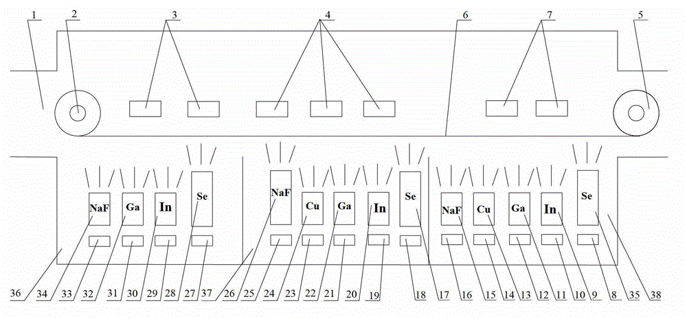
[0024] The preparation steps of the present invention, such as Figure 1-2 Shown:

[0025] Step 1: Preparation before work

[0026] The outer end of the whole roll of PI flexible substrate on the starting roller 2 in the vacuum chamber for preparing the absorbing layer is rolled onto the terminal roller 5 to form a roll-to-roll PI flexible substrate 6. After winding, the two The PI flexible substrate between the rollers forms a horizontal plane, and the side on which the back electrode Mo is deposited is facing down. In the film deposition chamber, the bottom of the back electrode Mo is the first process chamber (hereinafter referred to as the first chamber) 36 and the second chamber from left to right. The second process chamber (hereinaft...


PUM


Abstract

The invention relates to a method for manufacturing a sodium-doped absorbing layer on a reel-to-reel flexible polyimide (PI) substrate. The method is characterized by comprising the steps of 1 performing preparation before work, 2 preparing Na-doped indium gallium selenide (IGS) film, 3 preparing a copper-rich copper indium gallium selenide (CIGS) film; and 4 preparing the sodium-doped absorbing layer on the reel-to-reel flexible PI substrate. The method adopts a vacuum evaporation technology, keeps a distance between evaporation sources and the PI substrate to be 300-400mm and adjusts tape transporting speed of the PI substrate to enable the PI substrate to be lower than 450 DEG C, elements evaporated by the evaporation sources can be compounded on a back electrode Mo of the PI substrate well, and the Na-doped IGS film with even thickness is formed on the back electrode Mo. Due to the fact that Na atoms diffuse and enter the crystal boundary position of the IGS film to form a deep energy level defect, a foundation is laid for fully even Na doping into a large-area absorbing layer and strengthening of adhesion of the absorbing layer, and the effects of improving open-circuit voltage and electrical property of batteries are played.

Description

technical field [0001] The invention belongs to the technical field of copper indium gallium selenide thin film solar cells, and in particular relates to a method for preparing a sodium-doped absorbing layer on a roll-to-roll flexible PI substrate. Background technique [0002] As the energy crisis becomes more and more serious, people pay more and more attention to renewable energy. Among them, solar energy has become the most potential technology because of its inexhaustibility, cleanliness and pollution-free. Silicon-based solar technology is currently the most mature and has the highest market share, but it is not the most ideal solar technology due to the high energy consumption and high pollution preparation process. In recent years, thin-film solar technology has begun to rise. Since thin-film batteries have the advantages of light weight, low cost, and easy installation, they have developed rapidly once they were proposed. Among them, copper indium gallium selenium...

Claims


Application Information

Patent Timeline
Patent Type & Authority Applications(China)
IPC IPC(8): C23C14/24C23C14/56H01L31/18
CPCY02P70/50
Inventor 申绪男
Owner CHINA ELECTRONIC TECH GRP CORP NO 18 RES INST
Why Eureka
Try Eureka