Photoconductive semiconductor switch structure

A switch structure, semiconductor technology, applied in the direction of semiconductor devices, electrical components, circuits, etc., can solve the problems of current congestion between electrodes and semiconductor materials, reduction of the area of ​​photoconductive semiconductor switches, shortening the life of photoconductive semiconductor switches, etc., to reduce heat, reduce dark Current, the effect of reducing the current density

Inactive Publication Date: 2013-02-27
DONGGUAN WUFENG TECH
View PDF5 Cites 11 Cited by
  • Summary
  • Abstract
  • Description
  • Claims
  • Application Information

AI Technical Summary

Problems solved by technology

The disadvantage of the former is that it is difficult to prepare a high-quality passivation layer, while the latter is not an all-solid-state device and is not easy to use
[0005] At present, the breakdown voltage of the photoconductive semiconductor switch is much lower than that of its semiconductor material and the conduction current is small. The reasons are as follows: 1. The withstand voltage packaging technology of the switch needs to be improved, especially the insulation of the laser incident surface. Protection, which mainly involves the material selection and process technology of the passivation layer, but research shows that increasing the passivation layer will significantly shorten the life of the photoconductive semiconductor switch; 2. The ohmic contact technology between the metal electrode and the semiconductor material of the photoconductive semiconductor switch needs to be developed Improvement, if the bias voltage is too high or the conduction current is too large, the current density will also increase, resulting in current congestion and subsequent Joule heat between the electrode and the semiconductor material, which is prone to burnout; 3. The substrate material itself There are defects, such as micropipes, dislocations, small-angle grain boundaries and other defects. When the electric field at these defects is large, breakdown is easy to occur. The existence of defects directly limits the reduction of the area of ​​the photoconductive semiconductor switch, making it impossible to reduce the current. density

Method used


Image

  • Photoconductive semiconductor switch structure
  • Photoconductive semiconductor switch structure

Examples


Embodiment Construction

[0019] The present invention will be described in detail below in conjunction with the accompanying drawings.

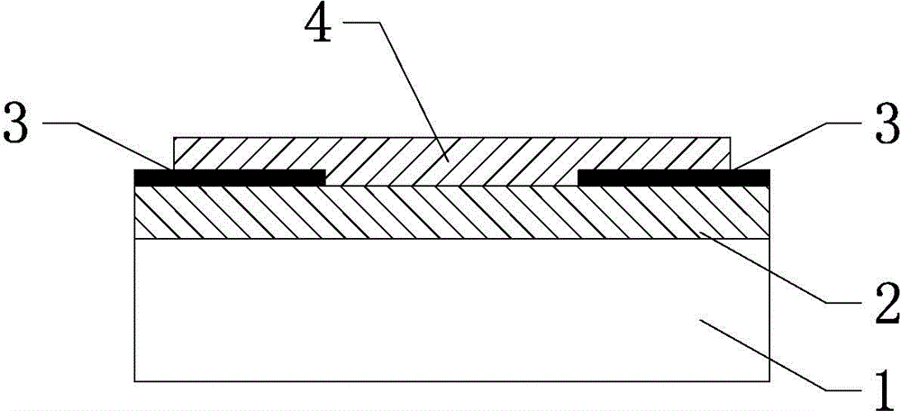
[0020] Such as figure 1 As shown, a photoconductive semiconductor switch structure of the present invention includes a substrate 1, the top surface of the substrate 1 is provided with a first silicon carbide film 2, and the two sides of the top surface of the first silicon carbide film 2 are respectively An electrode 3 is provided, and a second silicon carbide film 4 is provided on the top surface of the electrode 3 , and the second silicon carbide film 4 covers the gap between the electrodes 3 and a partial area of ​​the top surface of the electrode 3 . Compared with the traditional photoconductive semiconductor switch, the present invention is provided with a layer of second silicon carbide film 4 on the top surface of the electrode 3, and adopts a layer of second silicon carbide film 4 to cover the gap between the electrodes 3 and the part of the top surface of th...


PUM

PropertyMeasurementUnit
Resistivityaaaaaaaaaa

Abstract

The invention relates to the technical field of semiconductor apparatuses, and in particular relates to a photoconductive semiconductor switch structure. The photoconductive semiconductor switch structure comprises a substrate, wherein a first silicon carbide film is arranged on the top surface of the substrate; electrodes are respectively arranged on the two ends of the top end surface of the first silicon carbide film; a second silicon carbide film is arranged on the top end surfaces of the electrodes; and the second silicon carbide film covers a gap between the electrodes and part area on the top end surfaces of the electrodes. According to the photoconductive semiconductor switch structure disclosed by the invention, a silicon carbide film is arranged on the top end surfaces of the electrodes to increase the contact area of the silicon carbide film and the electrodes, so that break-over current can circulate from the two surfaces of the electrodes. Meanwhile, breakdown voltage and break-over current of the photoconductive semiconductor switch are improved, and the dark current is reduced.

Description

technical field [0001] The invention relates to the technical field of semiconductor devices, in particular to a photoconductive semiconductor switch structure. Background technique [0002] Photoconductive Semiconductor Switches (PCSS for short) is a semiconductor optoelectronic device that has developed rapidly in recent years. Its working principle is essentially to use the photoelectric effect of semiconductors to modulate the conductivity of semiconductor photoconductive materials. A certain bias voltage is applied to the electrode of the photoconductive semiconductor switch, and the laser pulse is irradiated on the semiconductor material of the switch to generate a large number of carriers. At this time, the switch is turned on and an output electric pulse is generated; The child disappears, the switch returns to the original blocking state, and the output electric pulse disappears. Compared with traditional switches, photoconductive semiconductor switches have many a...

Claims


Application Information

Patent Timeline
IPC IPC(8): H01L31/08H01L31/0224
Inventor 杨汇鑫胡刚
Owner DONGGUAN WUFENG TECH
Why Eureka
Try Eureka