Bottom-emitting organic electroluminescence device and preparation method thereof

A technology of electroluminescence and bottom emission, which is applied in the fields of electric solid-state devices, semiconductor/solid-state device manufacturing, electrical components, etc., and can solve the problems of complex process, affecting luminous efficiency, and poor control of doping ratio.

Inactive Publication Date: 2013-03-06
OCEANS KING LIGHTING SCI&TECH CO LTD +1
View PDF2 Cites 6 Cited by
  • Summary
  • Abstract
  • Description
  • Claims
  • Application Information

AI Technical Summary

Problems solved by technology

[0004] In traditional light-emitting devices, since the transport rate of electrons is two orders of magnitude lower than that of holes (the hole transport rate is generally 10 -3 cm 2 V -1 S -1 , the electron transfer rate is generally 10 -5 cm 2 V -1 S -1 ), this difference in rate often leads to a low probability of exciton recombination, which ultimately affects the luminous efficiency. Therefore, it is generally necessary to add an electron transport layer and an electron injection layer to increase the transmission and injection of electrons, so as to increase the recombination probability of excitons However, these functional layers have many evaporation processes, at least two layers (transport and injection) are required, and the injection layer is generally prepared by doping co-evaporation, the doping ratio is not easy to control, and the process is complicated, which ultimately makes the device The repeatability is not good, which is not conducive to industrial production

Method used


Image

  • Bottom-emitting organic electroluminescence device and preparation method thereof
  • Bottom-emitting organic electroluminescence device and preparation method thereof

Examples


preparation example Construction

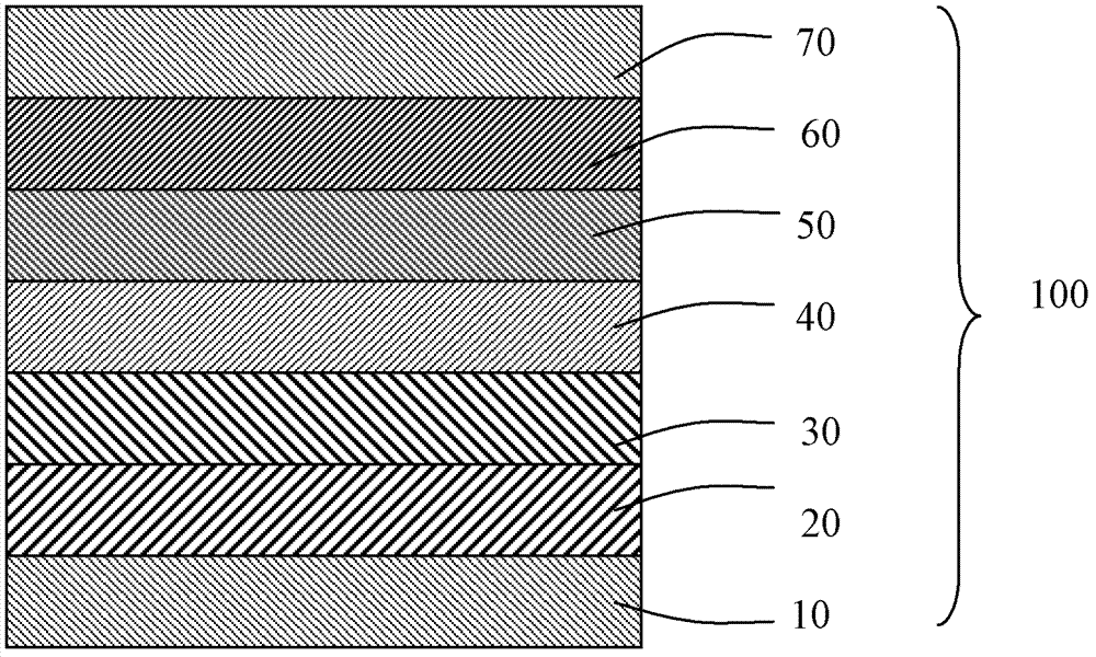
[0034] A method for preparing an organic electroluminescent device 100 according to an embodiment includes the following steps:

[0035] Step S110 , performing pretreatment on the conductive anode substrate 10 .

[0036]The conductive anode substrate 10 is preferably indium tin oxide glass (ITO), fluorine doped tin oxide glass (FTO), aluminum doped zinc oxide glass (AZO) or indium doped zinc oxide glass (IZO). Specifically, the anode conductive substrate 10 can be photolithographically processed first, cut into the required size, and then ultrasonicated for 15 minutes with detergent, deionized water, acetone, ethanol, and isopropanol in order to remove organic pollution on the glass surface Objects; after cleaning, carry out suitable treatment on the conductive substrate, such as: oxygen plasma treatment or UV-ozone treatment. The oxygen plasma treatment time is 5-15 minutes, and the power is 10-50 W; the UV-ozone treatment time is 5-20 minutes.

[0037] Step S120 , sequenti...

Embodiment 1

[0048] Example 1: First, carry out photolithography treatment on ITO, cut it into the required size, and then use detergent, deionized water, acetone, ethanol, and isopropanol to sonicate for 15 minutes each to remove organic pollutants on the glass surface; clean it up Carry out oxygen plasma treatment afterward, treatment time is 5min, and power is 35W, then vapor-deposits hole injection layer (MoO 3 ), hole transport layer (NPB), electron blocking layer (TAPC); 3 ); and then the electron beam prepares the sulfide layer, the material is ZnS, the thickness is 80nm, and finally the cathode is evaporated, the material is Ag, the thickness is 100nm, and finally the required organic electroluminescent device is obtained.

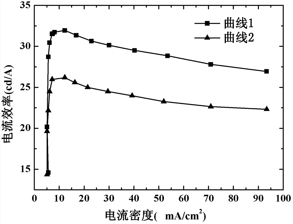
[0049] attached figure 2 The device structure of embodiment 1 is: ITO / MoO 3 / NPB / TAPC / Alq 3 / ZnS / Ag vs. voltage for conventional devices. Wherein, curve 1 is the result of embodiment 1, and curve 2 is the result of comparative example.

[0050] From fig...

Embodiment 2

[0051] Example 2: First, carry out photolithography treatment on FTO, cut it into the required size, and then use detergent, deionized water, acetone, ethanol, and isopropanol to sonicate for 15 minutes each to remove organic pollutants on the glass surface; clean it Carry out oxygen plasma treatment afterward, treatment time is 10min, power is 20W; Evaporate hole injection layer (WO 3 ), the hole transport layer (TCTA), the electron blocking layer (TPD); then evaporate the luminescent layer, the material is TCTA:FIrpic, the doping ratio is 20%, and the thickness is 20nm); then the electron beam prepares the sulfide layer, the material The material is CdS with a thickness of 10nm, and finally the cathode is evaporated, and the material is Al with a thickness of 100nm, and finally the required organic electroluminescent device is obtained.


PUM


Abstract

The invention relates to a bottom-emitting organic electroluminescence device and a preparation method of the bottom-emitting organic electroluminescence device. The bottom-emitting organic electroluminescence device comprises a conductive anode base, a hole injector layer, a hole transport layer, an electron barrier layer, a luminescent layer, a sulfide layer and a metal cathode which are sequentially stacked. According to the organic electroluminescence device, the sulfide layer is prepared to be used as an electron transport and injection function layer, a sulfide semiconductor belongs to an n-type semiconductor material, a relatively direct and complete conduction band path is provided for electron jump transmission, jump times of electrons in a transmission path is reduced, the migration rate of the electrons is further enhanced, and the transmission capacity of the electrons in the device is improved.

Description

【Technical field】 [0001] The invention relates to a bottom emission organic electroluminescence device and a preparation method thereof. 【Background technique】 [0002] In 1987, C.W.Tang and Van Slyke of Eastman Kodak Company in the United States reported a breakthrough in the research of organic electroluminescence. A high-brightness, high-efficiency double-layer small-molecule organic electroluminescent device was prepared using ultra-thin film technology. In this double-layer structure device, the brightness reaches 1000cd / m at 10V 2 , its luminous efficiency is 1.51lm / W, and its lifespan is more than 100 hours. In 1990, Burronghes et al. of the University of Cambridge proposed for the first time to use polymer conjugated polymer polyphenylene vinylene (PPV) to make polymer electroluminescence (EL) devices. Subsequently, the experimental group led by Professor Heeger of the University of California in the United States In 1991, the electroluminescent properties of poly...

Claims


Application Information

Patent Timeline
Patent Type & Authority Applications(China)
IPC IPC(8): H01L51/50H01L51/54H01L51/52
Inventor 周明杰王平黄辉钟铁涛
Owner OCEANS KING LIGHTING SCI&TECH CO LTD
Why Eureka
Try Eureka