
Prepreg, wiring board, and semiconductor device

A prepreg and wiring board technology, which is applied in the field of wiring boards, semiconductor devices and prepregs, can solve the problems of difficulty in satisfying the tightness of the embedded conductor layer, and it is difficult to form a fine circuit, so as to achieve connection The effect of excellent reliability, excellent installation reliability, and excellent adhesion

Inactive Publication Date: 2013-03-06
SUMITOMO BAKELITE CO LTD
View PDF4 Cites 29 Cited by
  • Summary
  • Abstract
  • Description
  • Claims
  • Application Information

AI Technical Summary

Problems solved by technology

In order to meet such demands, thinning of the prepreg constituting the wiring board has also been studied. However, when the prepreg is thinned, it is difficult to satisfy both embedding and adhesion to the conductor layer. , and it is difficult to form a fine circuit when the conductor is laminated on the prepreg

Method used


Image

  • Prepreg, wiring board, and semiconductor device
  • Prepreg, wiring board, and semiconductor device
  • Prepreg, wiring board, and semiconductor device

Examples


Embodiment 1)

[0173] 1. Preparation of the first epoxy resin composition

[0174] 30 parts by weight of naphthalene-modified cresol novolac epoxy resin (manufactured by DIC Corporation, HP-5000) as an epoxy resin, biphenyl aralkyl type phenolic resin as a phenol curing agent (manufactured by Meiwa Chemical Co., Ltd., MEH7851- 5H) 20 parts by weight of phenoxy resin (manufactured by jER Corporation, YX-8100BH30, 30% by weight of solid content) as a thermoplastic resin, with a solid content of 30 parts by weight, as an average particle size of silica nanoparticles of 1 to 100 nm 20 parts by weight of spherical silica (manufactured by TOKUYAMA Co., Ltd., NSS-5N) with a diameter of 75 nm, and 0.5 parts by weight of imidazole (manufactured by Shikoku Chemicals, Inc., Curezol 2E4MZ) as a curing agent were mixed and dissolved in methyl ethyl ketone, and the non-volatile content was adjusted to 45 parts by weight. %, the first epoxy resin composition was prepared.

[0175] 2. Preparation of the 2n...

Embodiment 2)

[0190] In the preparation of the first epoxy resin composition, instead of using biphenyl aralkyl type phenolic resin and Curezol 2E4MZ, 20 wt. and Curezol 1B2PZ (manufactured by Shikoku Chemical Industry Co., Ltd.) 0.3 parts by weight, except that it is the same as in Example 1.

Embodiment 3)

[0192] In the preparation of the first epoxy resin composition, instead of using a naphthalene-modified cresol novolak epoxy resin, 30 parts by weight of an anthracene-type epoxy resin (manufactured by jER, YX-8800) was used. Example 2 is the same.


PUM

PropertyMeasurementUnit
Thicknessaaaaaaaaaa
Thicknessaaaaaaaaaa
Thicknessaaaaaaaaaa

Abstract

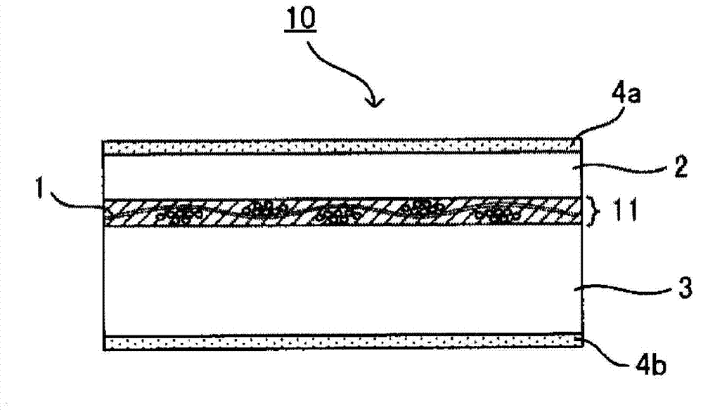
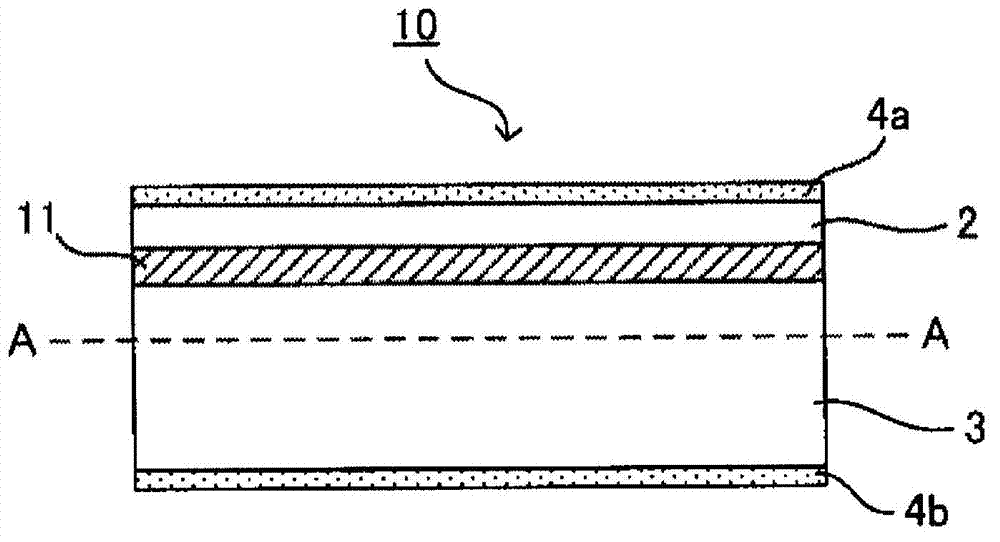
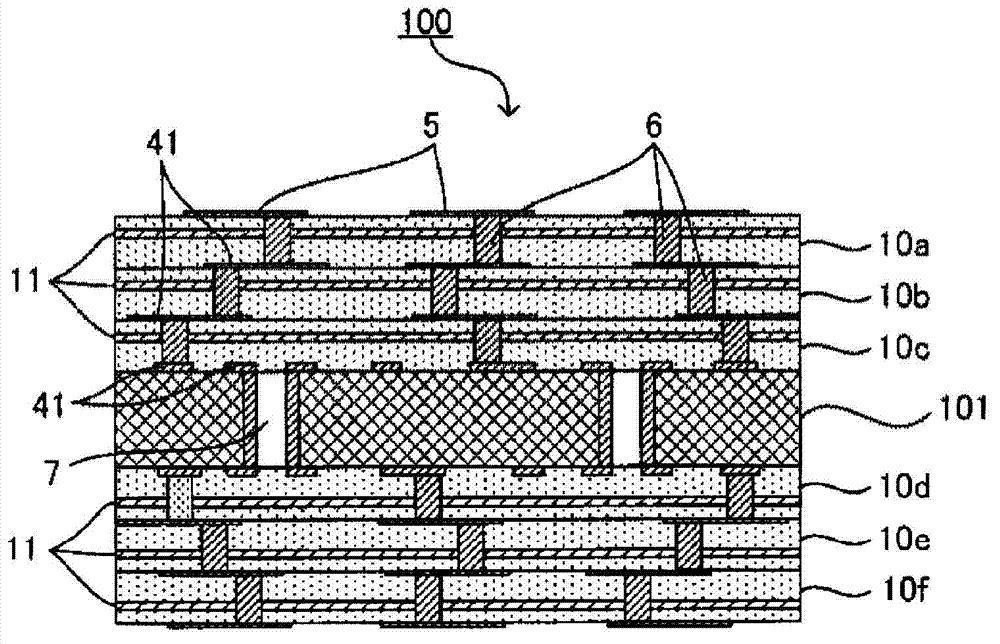
Provided is a prepreg which can accommodate a thickness reduction and in which different applications, functions, performances, characteristics, or the like can be imparted respectively to the two surfaces thereof. One of the surfaces of the prepreg has excellent adhesion to a conductor layer, and a fine circuit can be formed thereon. The prepreg comprises a core layer equipped with a fibrous base, a first resin layer, and a second resin layer and further includes a carrier film laminated to the surface of the first resin layer and / or the surface of the second resin layer. The prepreg is characterized in that the first resin layer is a layer comprising a first epoxy resin composition which comprises silica nanoparticles having an average particle diameter of 1-100 nm, a thermoplastic resin, and an epoxy resin, the first resin layer being in contact with the fibrous base or some of the first resin layer having been infiltrated into the fibrous base, and that the second resin layer comprises a second epoxy resin composition which comprises an inorganic filler and an epoxy resin, some of the second resin layer having been infiltrated into the fibrous base.

Description

technical field [0001] The present invention relates to a prepreg, a wiring board, and a semiconductor device. [0002] this application claims priority based on Japanese Patent Application No. 2010-151259 for which it applied to Japan on July 1, 2010, and uses the content here. Background technique [0003] A wiring board (circuit board) is generally formed by impregnating a thermosetting resin into a glass fiber substrate or the like to obtain a prepreg, laminating several prepregs, heating and pressing. In addition, the prepreg is obtained by a method of impregnating a glass fiber base material having a thickness of about 50 to 200 μm in a thermosetting resin composition (varnish) or the like (for example, refer to Patent Document 1). [0004] In some cases, prepregs require embedding properties in gaps for embedding circuit wiring on one side, and require adhesion to conductor layers for forming circuits on the other side. However, in the prepreg obtained by the conven...

Claims


Application Information

Patent Timeline
IPC IPC(8): C08J5/24B32B5/28B32B27/12H05K1/03
CPCH05K2201/029H05K1/02H05K3/4655H05K3/4602H05K2201/0129C08J2363/00C08J5/24B32B17/04B32B19/02H05K2201/0358H05K2201/0195H05K1/0366H05K2201/0209H01L2224/16227Y10T428/24355Y10T428/252Y10T428/2495C08J5/244C08J5/249B32B27/12H05K1/03B32B5/24C08K3/36C08J2300/22C08K2201/005C08K2201/011
Inventor 大东范行远藤忠相
Owner SUMITOMO BAKELITE CO LTD
Learn More