

Nitride high electronic mobility transistor extension structure of component gradually-changed ALyGal-yN buffer layer
A technology with high electron mobility and gradual change in composition, which is applied in the direction of circuits, electrical components, semiconductor devices, etc., can solve the problems that affect the application potential of GaNHEMT in the direction of high power, the decrease of device output power, and the decrease of efficiency, so as to reduce the self-heating effect, Effect of reducing dislocations and improving thermal conductivity
- Summary
- Abstract
- Description
- Claims
- Application Information
AI Technical Summary
Problems solved by technology
Method used
Image

Examples
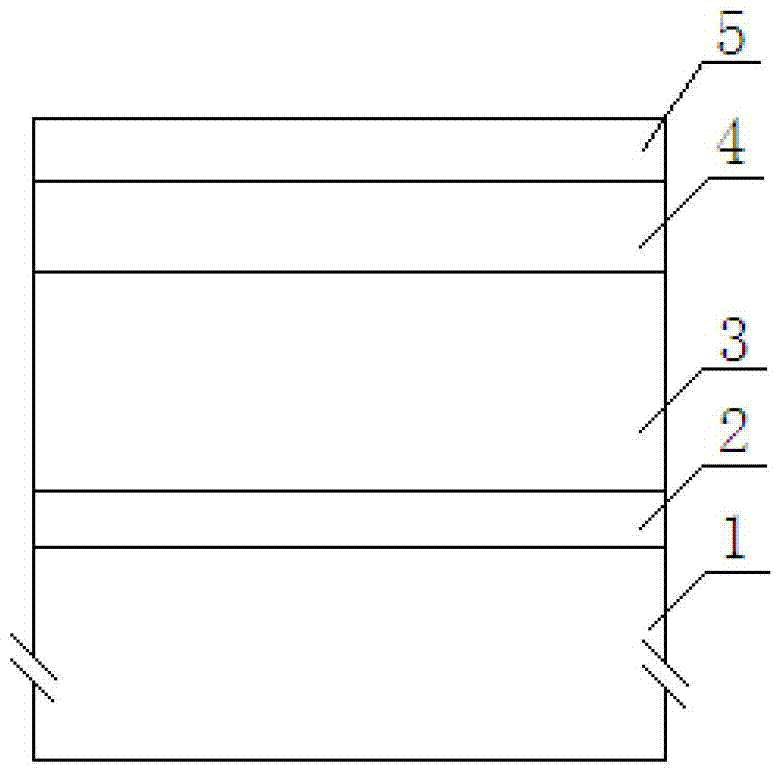
Embodiment 1
[0015] 1) Select a sapphire substrate and grow it using MOCVD technology;
[0016] 2) Baking at 1080°C and 100Torr in a hydrogen atmosphere for 5 minutes;
[0017] 3) Cool down to 550°C, inject ammonia gas and trimethylgallium, and grow a 20nm thick GaN nucleation layer on the substrate surface;
[0018] 4) Introduce ammonia, trimethylaluminum and trimethylgallium to grow 2.0um thick composition gradient Al y Ga 1-y N, Al composition y gradually changes from 0 to 0.04 from bottom to top;
[0019] 5) Turn off trimethylaluminum, grow 200nm thick GaN channel layer at 1080°C;
[0020] 6) Open trimethylaluminum again, and grow a 25nm thick AlGaN barrier layer;
[0021] 7) Cool down to room temperature.
Embodiment 2
[0023] 1) Select the SiC substrate and grow it using MOCVD technology;
[0024] 2) Baking at 1080°C and 100Torr in a hydrogen atmosphere for 10 minutes;
[0025] 3) At 1150°C, inject ammonia gas and trimethylaluminum, and grow a 50nm thick AlN nucleation layer on the substrate surface;
[0026] 4) Introduce ammonia, trimethylaluminum and trimethylgallium to grow 2.5um thick composition gradient Al y Ga 1-y N, Al composition gradually changes from 0 to 0.05 from bottom to top;
[0027] 5) Turn off trimethylaluminum, grow 100nm thick GaN channel layer at 1080°C;
[0028] 6) Open trimethylaluminum again, grow 1nm thick AlN and 20nm thick AlGaN barrier layer at 1080°C;
[0029] 7) Cool down to room temperature.
Embodiment 3
[0031] 1) Select a single crystal Si substrate and grow it using MOCVD technology;
[0032] 2) Baking at 1100°C and 100Torr in a hydrogen atmosphere for 10 minutes;
[0033] 3) Lower the temperature to 1060°C, pass through trimethylaluminum for 30 seconds, and form an Al layer on the surface of the Si substrate;
[0034] 4) A 300nm-thick AlN nucleation layer is grown by injecting ammonia gas and trimethylaluminum;
[0035] 5) Introduce ammonia, trimethylaluminum and trimethylgallium to grow 2.5um thick composition gradient Al y Ga 1-y N, Al composition y gradually changes from 0 to 0.06 from bottom to top;
[0036] 6) Turn off trimethylaluminum, grow 500nm thick GaN channel layer at 1080°C;
[0037] 7) Open trimethylaluminum again, grow 25nm thick AlGaN barrier layer at 1100°C;
[0038] 8) Cool down to room temperature.
PUM
| Property | Measurement | Unit |
|---|---|---|
| Thickness | aaaaa | aaaaa |
| Thickness | aaaaa | aaaaa |
Abstract
Description
Claims
Application Information