Ultraviolet light-emitting diode with transparent zinc oxide base conducting layer and fabrication method of ultraviolet light-emitting diode

A transparent conductive layer, light-emitting diode technology, applied in circuits, electrical components, semiconductor devices, etc., can solve the problems of chip heating, chip life impact, low LED light extraction efficiency, etc., to achieve uniform current diffusion and reduce the probability of total internal reflection , the effect of improving light extraction efficiency

Inactive Publication Date: 2013-03-20
SOUTHEAST UNIV
View PDF3 Cites 11 Cited by
  • Summary
  • Abstract
  • Description
  • Claims
  • Application Information

AI Technical Summary

Problems solved by technology

The main reason for the low light extraction efficiency of LEDs is the total internal reflection of light at the interface between semiconductor materials and air.
Total internal reflection has at least two adverse effects on the performance of the LED chip: on the one hand, it reduces the light extraction efficiency of the LED chip; severe impact

Method used


Image

  • Ultraviolet light-emitting diode with transparent zinc oxide base conducting layer and fabrication method of ultraviolet light-emitting diode
  • Ultraviolet light-emitting diode with transparent zinc oxide base conducting layer and fabrication method of ultraviolet light-emitting diode

Examples


Embodiment Construction

[0027] The present invention will be further described below in conjunction with the accompanying drawings and embodiments of the specification.

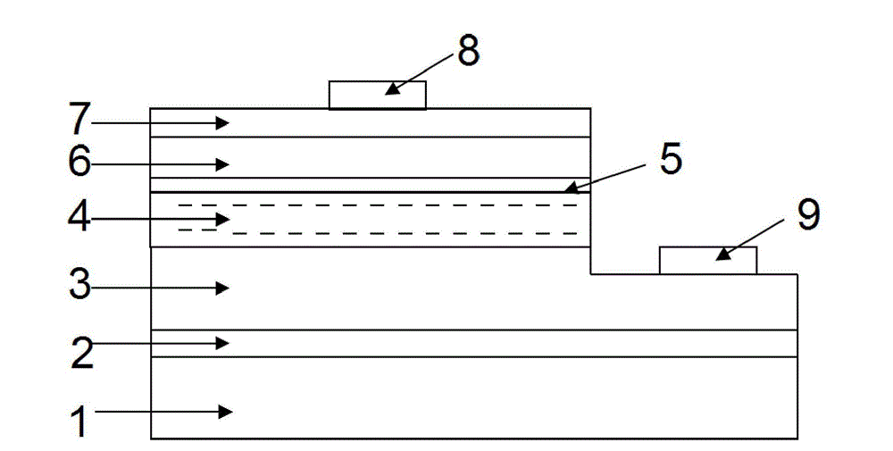
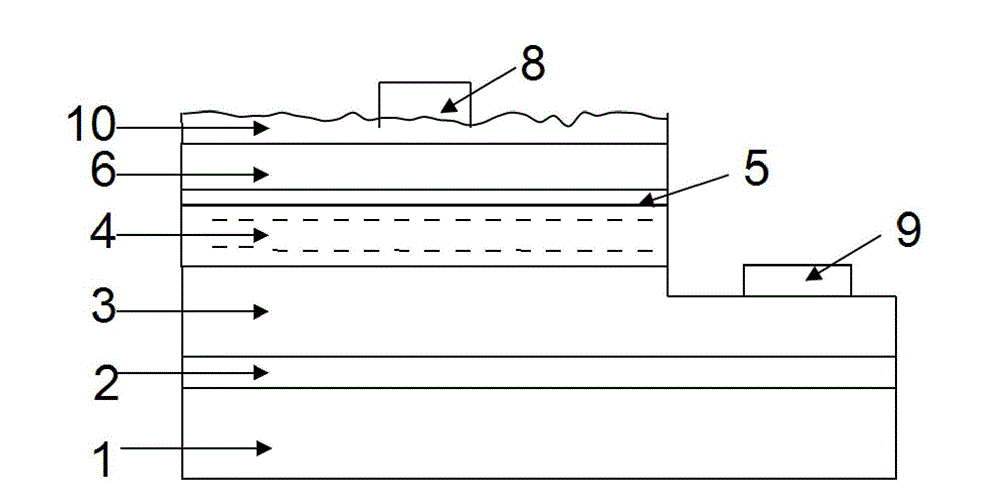
[0028] The ultraviolet light-emitting diode chip with a zinc oxide-based transparent conductive layer of the present invention includes a sapphire substrate 1, an aluminum nitride buffer layer 2, an n-type aluminum gallium nitride layer 3, and an aluminum gallium nitrogen multiquantum well layer connected sequentially from bottom to top. Source layer 4, p-type aluminum gallium nitride electron blocking layer 5, p-type gallium nitride layer 6, zinc oxide-based transparent conductive layer 10, p-type metal electrode 8 on the zinc oxide-based transparent conductive layer 10, n-type aluminum gallium Part of the upper surface of the nitrogen layer 3 is connected to the lower surface of the AlGaN MQW active layer 4 , and an n-type metal electrode 9 is provided in the area not connected to the AlGaN MQW active layer 4 .

[0029] In one emb...


PUM

PropertyMeasurementUnit
Thicknessaaaaaaaaaa

Abstract

The invention discloses an ultraviolet light-emitting diode chip with a transparent conducting layer, and a fabrication method of the ultraviolet light-emitting diode chip. The chip comprises a sapphire substrate, an aluminum nitride buffer layer, an n-type aluminum gallium nitrogen layer, an aluminum gallium nitrogen multiple quantum well active layer, a p-type aluminum gallium nitrogen electron barrier layer, a p-type gallium nitride layer, a transparent zinc oxide base conducting layer, a p-type metal electrode on the transparent zinc oxide base conducting layer, and an n-type metal electrode on the n-type aluminum gallium nitrogen layer. The fabrication method adopts a metallorganics chemical vapor deposition method and a pulsed laser deposition method. The ultraviolet light-emitting diode chip has the advantages of low resistivity and high ultraviolet light transmittance; and fabrication raw materials are rich, low in price and environment-friendly.

Description

technical field [0001] The invention belongs to the technical field of light emitting diode (LED, Light Emitting Diode) chips, and relates to an ultraviolet LED chip with a ZnO-based transparent conductive layer and a preparation method thereof. Background technique [0002] As a new type of high-efficiency solid-state light source, LED has significant advantages such as energy saving, environmental protection, long life, small size, and low voltage, and has been widely used in the world. Among them, ultraviolet LEDs with a wavelength of 210-360nm have a wide range of application potentials in the fields of air purification, biomedicine, and information security due to their high modulation frequency, low noise, environmental protection, and high-efficiency sterilization potential. [0003] The ultraviolet LED chip requires the current diffusion layer to have a high ultraviolet light transmittance (T>80%) and a low resistivity (ρ<10-4Ω·cm). The commonly used and comme...

Claims


Application Information

Patent Timeline
IPC IPC(8): H01L33/14H01L33/22H01L33/00
Inventor 张雄王书昶崔一平
Owner SOUTHEAST UNIV
Why Eureka
Try Eureka