

High-efficiency organic light-emitting diode and fabrication method thereof
A light-emitting diode, high-efficiency technology, used in semiconductor/solid-state device manufacturing, electrical components, electrical solid-state devices, etc., can solve problems such as reducing the optical coupling output efficiency of the device, and achieve higher efficiency, improved spectral purity, and improved device spectrum. Effect
- Summary
- Abstract
- Description
- Claims
- Application Information
AI Technical Summary
Problems solved by technology
Method used
Image

Examples
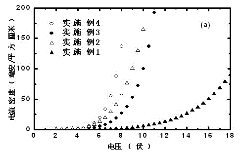
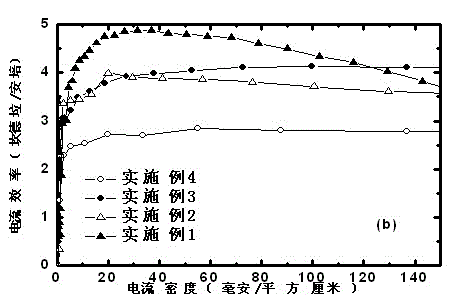
Embodiment 1
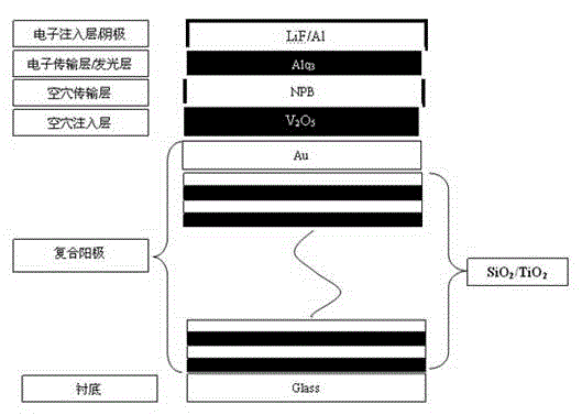
[0047] First clean the glass substrate with DBR, dry it with nitrogen, put the glass in a vacuum oven and bake it at 120 degrees Celsius for 30 minutes, then treat it with oxygen plasma for 2 minutes, and then put the glass in the vacuum coating system. When the vacuum degree of the vacuum coating system reaches 3×10 -4 At the time of Pa, Au with a width of 4 mm and a length of 30 mm was evaporated on a glass substrate with a DBR as an anode. Vapor-deposited on the anode sequentially 2 o 5 hole injection layer of NPB, hole transport layer of NPB, Alq 3 The light-emitting layer and electron transport layer of LiF, the electron injection layer of LiF and the cathode of metal Al, wherein the two electrodes intersect each other to form the light-emitting area of the device, the area of the light-emitting area is 16 square millimeters, the anode, the hole interface layer, the hole transport Layer, light-emitting layer and electron transport layer, electron interface layer a...
Embodiment 2
[0049] First, the ITO anode on the glass substrate with DBR / ITO is photolithographically formed into an electrode with a width of 4 mm and a length of 30 mm, cleaned, dried with nitrogen, and the glass is placed in a vacuum oven and baked at 120 degrees Celsius for 30 minutes. After that, it was treated with oxygen plasma for 2 minutes, after which, the glass was put into a vacuum coating system. When the vacuum degree of the vacuum coating system reaches 3×10 -4 Pa, sequentially vapor-deposit V on the anode 2 o 5 hole injection layer of NPB, hole transport layer of NPB, Alq 3 The light-emitting layer and electron transport layer of LiF, the electron injection layer of LiF and the cathode of metal Al. The intersecting part of the two electrodes forms the light-emitting area of the device. The area of the light-emitting area is 16 square millimeters. The hole interface layer, hole transport layer, The thicknesses of the light-emitting layer and the electron transport lay...
Embodiment 3
[0051] First clean the ordinary glass substrate, dry it with nitrogen, put the glass in a vacuum oven and bake it at 120 degrees Celsius for 30 minutes, then treat it with oxygen plasma for 2 minutes, and then put the glass into the vacuum coating system middle. When the vacuum degree of the vacuum coating system reaches 3×10 -4 At the time of Pa, first vapor-deposit Au with a width of 4 mm and a length of 30 mm on a common glass substrate as an anode. Vapor-deposited on the anode sequentially 2 o 5 hole injection layer of NPB, hole transport layer of NPB, Alq 3 The light-emitting layer and electron transport layer of LiF, the electron injection layer of LiF and the cathode of metal Al, wherein the two electrodes intersect each other to form the light-emitting area of the device, the area of the light-emitting area is 16 square millimeters, the anode, the hole interface layer, the hole transport Layer, light-emitting layer and electron transport layer, electron interfa...
PUM
 Abstract
Description
Claims
Application Information