Sacrificial layer of MEMS (Micro-Electro-Mechanical-System) device, MEMS device and manufacturing method thereof

A manufacturing method and sacrificial layer technology, applied in the field of sacrificial layers, can solve problems such as contamination of the chamber and easy decomposition of the sacrificial layer, and achieve the effects of high viscosity, large material selection range, and easy planarization

Inactive Publication Date: 2013-04-03
SHANGHAI HUAHONG GRACE SEMICON MFG CORP
View PDF8 Cites 9 Cited by
  • Summary
  • Abstract
  • Description
  • Claims
  • Application Information

AI Technical Summary

Problems solved by technology

[0008] The problem solved by the present invention is to propose a sacrificial layer to solve the problem that the sacrificial layer of the existing MEMS device is easy to decompose, thereby causing the problem of contaminating the chamber

Method used


Image

  • Sacrificial layer of MEMS (Micro-Electro-Mechanical-System) device, MEMS device and manufacturing method thereof
  • Sacrificial layer of MEMS (Micro-Electro-Mechanical-System) device, MEMS device and manufacturing method thereof
  • Sacrificial layer of MEMS (Micro-Electro-Mechanical-System) device, MEMS device and manufacturing method thereof

Examples


Embodiment 1

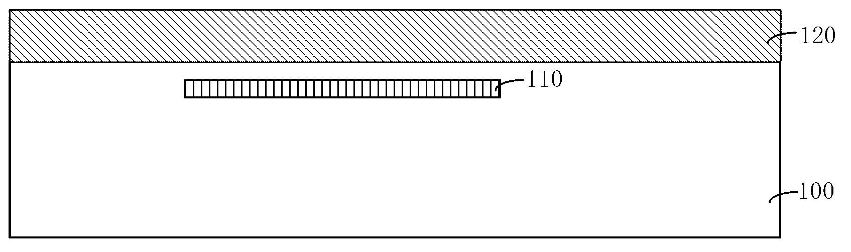
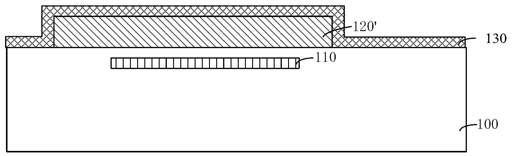
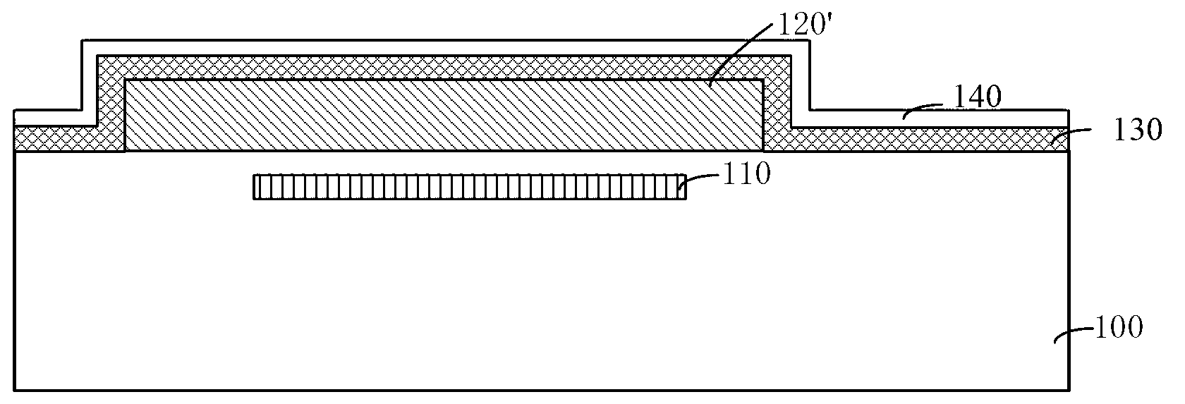
[0036] Figure 1 to Figure 5 Shown is a schematic structural diagram of the manufacturing method of the MEMS pressure sensor provided in this embodiment. The following combination Figure 1 to Figure 5 , through the fabrication method of the MEMS pressure sensor, the technical solution of the sacrificial layer provided by the present invention is introduced in detail.

[0037] Execute step S11: if figure 1 As shown, a semiconductor substrate 100 is provided, and a fixed electrode 110 is formed on the semiconductor substrate 100 . The fixed electrode 110 can be made of metal, or can be made of a semiconductor material containing a dopant (such as silicon material containing germanium). Of course, the fixed electrode 110 can also be made of other conductive materials. In addition, when active components, passive components or metal interconnection layers are formed in the semiconductor substrate 100 , the corresponding conductive components can also be used as the fixed electr...

Embodiment 2

[0053] The sacrificial layer of the MEMS pressure sensor provided in the second embodiment, the MEMS pressure sensor and its manufacturing method are substantially the same as those in the first embodiment. The difference is that the covering layer in the sacrificial layer is made of low temperature oxide (Low Temperature Oxide, LTO) instead of SOG. The low-temperature oxide is a kind of oxide, which can withstand high temperature, and its formation temperature is relatively low, generally not higher than 200°C. The low-temperature oxide can also isolate the organic material layer 120 from the pattern structure material when the pattern structure material is subsequently deposited on it, avoiding the high temperature of the deposition process to cause the organic material to decompose and escape, thereby achieving the goal of avoiding contamination of the deposition. The purpose of accumulating process chambers.

[0054] It can be understood that the MEMS pressure sensor is u...


PUM


Abstract

Different from the scheme that an organic material layer is separately used as a sacrificial layer of an MEMS (Micro-Electro-Mechanical-System) device, the invention adopts the following scheme that after the organic material layer is patterned, a covering layer with the decomposition temperature higher than that of the organic material layer covers the surface of the patterned organic material layer, so that a subsequent deposited structural material layer is isolated from the organic material layer to play a role of preventing a machine cavity from being polluted due to the decomposition and escape of the organic material layer in the high-temperature deposition process. In addition, the covering layer provides a larger material selection range for the organic material layer. Based on the sacrificial layer, the invention also provides the MEMS device comprising the sacrificial layer and a manufacturing method of the MEMS device.

Description

technical field [0001] The invention relates to the field of semiconductor manufacturing, in particular to a sacrificial layer of a MEMS device, the MEMS device and a manufacturing method thereof. Background technique [0002] In recent years, with the development of Micro-Electro-Mechanical-System (MEMS) technology, various micro-electro-mechanical devices, including: micro-sensors, micro-actuators, etc., have achieved miniaturization, which is beneficial to Improving the integration of devices has become the main direction of future development. [0003] The early MEMS process was based on the bulk silicon process, that is, the silicon wafer was etched to form structures such as cantilever beams. For more information about bulk silicon MEMS devices, please refer to the US patent publication number US6170332B1. [0004] However, the aforementioned bulk silicon process is not compatible with existing CMOS processes. In response to the above problems, the surface silicon pr...

Claims


Application Information

Patent Timeline
Patent Type & Authority Applications(China)
IPC IPC(8): B81B7/00B81C1/00
Inventor 黎坡
Owner SHANGHAI HUAHONG GRACE SEMICON MFG CORP
Why Eureka
Try Eureka