Interface conversion module of spaceborne electronic system

An electronic system and interface conversion technology, applied in the direction of electrical digital data processing, instruments, etc., can solve the problems of SpaceWire signal 485 signal and 422 signal can not be converted to each other, poor compatibility, etc., to promote modular design, reduce design costs, promote The effect of resource sharing

Active Publication Date: 2013-04-03
赛德雷特(珠海)航天科技有限公司
2 Cites 5 Cited by

AI-Extracted Technical Summary

Problems solved by technology

[0004] In order to solve the problem that SpaceWire signal and CAN signal, 485 signal and 422 signal cannot be mutually converted and th...

Abstract

The invention relates to an interface conversion module of a spaceborne electronic system, which belongs to the technical field of spaceflight data processing, and solves the problems in the prior art that a SpaceWire signal cannot be mutually converted with a CAN signal, a 485 signal and a 422 signal, and the compatibility is poor. After the interface conversion module is electrified, a single chip microcomputer reads a configuration file prestored in a FLASH internal memory, and an FPGA module based on a static random memory is configured through an FPGA configuration port. In the data conversion and transmission process, a signal conversion circuit and a routing circuit continuously output heartbeat signals with a certain period and pulse width and a monitoring circuit constantly monitors whether an abnormal phenomenon exists not. When the output pulse signal is often high and often low or irregular on the period, the monitoring circuit reports the abnormal phenomenon to a state control circuit, the state control circuit sends a control signal to an off-chip single chip microcomputer to command the single chip microcomputer to read the configuration code stream in the FLASH internal memory, and the FPGA module is reconfigured through the FPGA configuration port.

Application Domain

Electric digital data processing

Technology Topic

Data conversionData processing +11

Image

  • Interface conversion module of spaceborne electronic system

Examples

  • Experimental program(7)

Example Embodiment

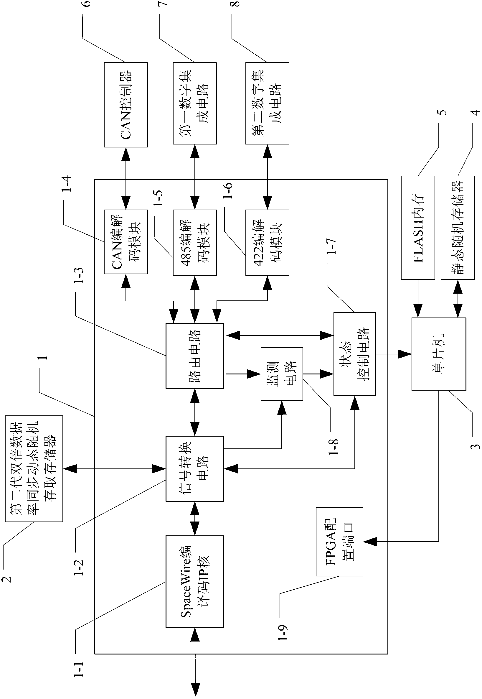
[0028] Specific implementation mode 1. Combination figure 1 Specifically illustrate the present embodiment, the on-board electronic system interface conversion module described in the present embodiment, it comprises the FPGA module 1 based on SRAM, the second generation double data rate synchronous DRAM 2, single-chip microcomputer 3, static Random access memory 4 and FLASH memory 5, described FPGA module 1 based on static random access memory comprises SpaceWire codec IP core 1-1, signal conversion circuit 1-2, routing circuit 1-3, CAN codec module 1-4, 485 codec module 1-5, 422 codec module 1-6, state control circuit 1-7, monitoring circuit 1-8 and FPGA configuration port 1-9,
[0029] The signal conversion circuit 1-2 has a total of: three data signal input and output terminals, one heartbeat signal output terminal and one buffer signal terminal,
[0030] Routing circuits 1-3 have a total of: five data signal input and output terminals and one heartbeat signal output terminal,
[0031] State control circuits 1-7 have a total of: two data signal input and output terminals, one data signal input terminal and one control signal output terminal,
[0032] The monitoring circuits 1-8 have a total of: two heartbeat signal input terminals and one data signal output terminal,
[0033] The MCU 3 has a total of: a configuration signal output terminal, a control signal input terminal, a data signal input terminal and a data signal input and output terminal;
[0034] The data signal input and output terminals of the CAN codec module 1-4 are connected with the first data terminal of the routing circuit 1-3,
[0035] The data signal input and output terminals of the 485 codec module 1-5 are connected with the second data terminal of the routing circuit 1-3,
[0036] The data signal input and output terminals of the 422 codec module 1-6 are connected to the third data terminal of the routing circuit 1-3,
[0037] The heartbeat signal output end of the routing circuit 1-3 is connected to the first heartbeat signal input end of the monitoring circuit 1-8,
[0038] The fourth data signal input and output end of the routing circuit 1-3 is connected to the first data signal input and output end of the state control circuit 1-7,
[0039] The fifth data signal input and output end of the routing circuit 1-3 is connected to the first data signal input and output end of the signal conversion circuit 1-2,
[0040] The buffer signal end of the signal conversion circuit 1-2 is connected with the buffer signal end of the second generation double data rate synchronous dynamic random access memory 2,
[0041] The second data signal input and output end of signal conversion circuit 1-2 is connected with the data signal input and output end of SpaceWire encoding and decoding IP core 1-1,
[0042] The third data signal input and output terminals of the signal conversion circuit 1-2 are connected with the data signal input and output terminals of the state control circuit 1-7,
[0043] The heartbeat signal output end of the signal conversion circuit 1-2 is connected with the second heartbeat signal input end of the monitoring circuit 1-8,
[0044] The data signal output end of the monitoring circuit 1-8 is connected with the data signal input end of the state control circuit 1-7,
[0045] The control signal output end of state control circuit 1-7 is connected with the control signal input end of single-chip microcomputer 3,
[0046] The data signal input end of single-chip microcomputer 3 is connected with the data signal input end of FLASH memory 5,
[0047] The data signal input and output terminals of the single-chip microcomputer 3 are connected with the data signal input and output terminals of the SRAM 4,
[0048] The configuration signal output end of the single-chip microcomputer 3 is connected with FPGA configuration ports 1-9.
[0049] The FPGA module 1 based on the SRAM of the present embodiment selects XC4VFX12 of Xilinx Company, and based on the internal circuit logic of the FPGA module 1 based on the SRAM, all are realized by hardware description language configuration. After power-on, the microcontroller 3 reads the pre-existing FLASH memory The configuration file in 5 configures FPGA module 1 based on SRAM through FPGA configuration ports 1-9. In the process of data conversion and transmission, the signal conversion circuit 1-2 and the routing circuit 1-3 are the two most critical functional parts, so they will continuously output a certain cycle and pulse through the I/O port during operation. The wide pulse signal, i.e. the heartbeat signal, is constantly monitored by the monitoring circuit 1-8 to see if there is any abnormality. If it is found that the output pulse signal is often high, often low or irregular in cycle, it indicates that the health state is abnormal. At this time, the monitoring circuit 1-8 reports the abnormality to the state control circuit 1-7, and the state control circuit 1-7 reports the abnormality to the off-chip The single-chip microcomputer 3 sends a control signal, commands the single-chip microcomputer 3 to read the configuration code stream in the FLASH memory 5, and reconfigures the FPGA through the FPGA configuration ports 1-9.

Example Embodiment

[0050] Specific embodiment two, combine figure 1 Specifically illustrate this embodiment, the difference between this embodiment and the on-board electronic system interface conversion module described in the first embodiment is that it also includes a CAN controller 6, and the data signal input and output terminals of the CAN controller 6 are connected to the The data signal input and output ends of the CAN codec modules 1-4 are connected.
[0051]The CAN data stream in this embodiment is set by the SJA1000 on parameters such as the code rate and clock frequency division, and then input to the on-chip CAN codec module 1-4, decoded to obtain the CAN data frame, and transmit it to the routing circuit 1-3, and the routing circuit 1-3 assigns ports and transmits them to the signal conversion circuit 1-2. The signal conversion circuit 1-2 converts the CAN data frame into a data frame conforming to the SpaceWire protocol, and finally encodes and outputs the IP core 1-1 through SpaceWire encoding and decoding.
[0052] The SpaceWire data stream is input to the on-chip SpaceWire encoding and decoding IP core 1-1. After decoding, the valid data is taken out by the signal conversion circuit 1-2, converted into CAN data frames, and distributed to the CAN interface circuit for output through the routing circuit 1-3. Among them, in order to match the high-speed code rate and the low-speed code rate, the second-generation double data rate synchronous dynamic random access memory 2 is used for data buffering.

Example Embodiment

[0053] Specific embodiment three, combine figure 1 Describe this embodiment in detail. The difference between this embodiment and the on-board electronic system interface conversion module described in the first embodiment is that it also includes a first digital integrated circuit 7, and the data signal of the first digital integrated circuit 7 The input and output ends are connected with the data signal input and output ends of the 485 encoding and decoding modules 1-5.

PUM

no PUM

Description & Claims & Application Information

We can also present the details of the Description, Claims and Application information to help users get a comprehensive understanding of the technical details of the patent, such as background art, summary of invention, brief description of drawings, description of embodiments, and other original content. On the other hand, users can also determine the specific scope of protection of the technology through the list of claims; as well as understand the changes in the life cycle of the technology with the presentation of the patent timeline. Login to view more.

Similar technology patents

Method and device for decoding data streams

InactiveCN105828083ASimple circuit structureSave FPGA resources
Owner:ZTE CORP

Classification and recommendation of technical efficacy words

  • Simple circuit structure
  • Reduce design cost

DDS signal generator and frequency hopping method

ActiveCN102468868AReduce design costGood scalability and upgradeability
Owner:SUZHOU RIGOL PRECISION ELECTRIC TECH
Why Eureka
Try Eureka