Field effect transistor of radio frequency lateral double-diffusion and preparation method thereof

A field effect transistor and lateral double diffusion technology, which is applied in the manufacture of the transistor and the field of radio frequency lateral double diffusion field effect transistors, can solve the problems of complex process, reduce the electric field strength, reduce the metal deposition process, high breakdown The effect of voltage

Active Publication Date: 2013-04-10
SHANGHAI HUAHONG GRACE SEMICON MFG CORP
View PDF4 Cites 6 Cited by
  • Summary
  • Abstract
  • Description
  • Claims
  • Application Information

AI Technical Summary

Problems solved by technology

However, the two-layer Faraday shield structure of the traditional RFLDMOS

Method used


Image

  • Field effect transistor of radio frequency lateral double-diffusion and preparation method thereof
  • Field effect transistor of radio frequency lateral double-diffusion and preparation method thereof
  • Field effect transistor of radio frequency lateral double-diffusion and preparation method thereof

Examples


Embodiment Construction

[0052] In order to enable your examiners to have a further understanding and understanding of the objects, features and effects of the present invention, the following detailed descriptions are given in conjunction with the accompanying drawings.

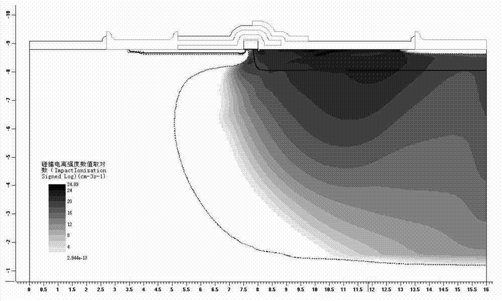
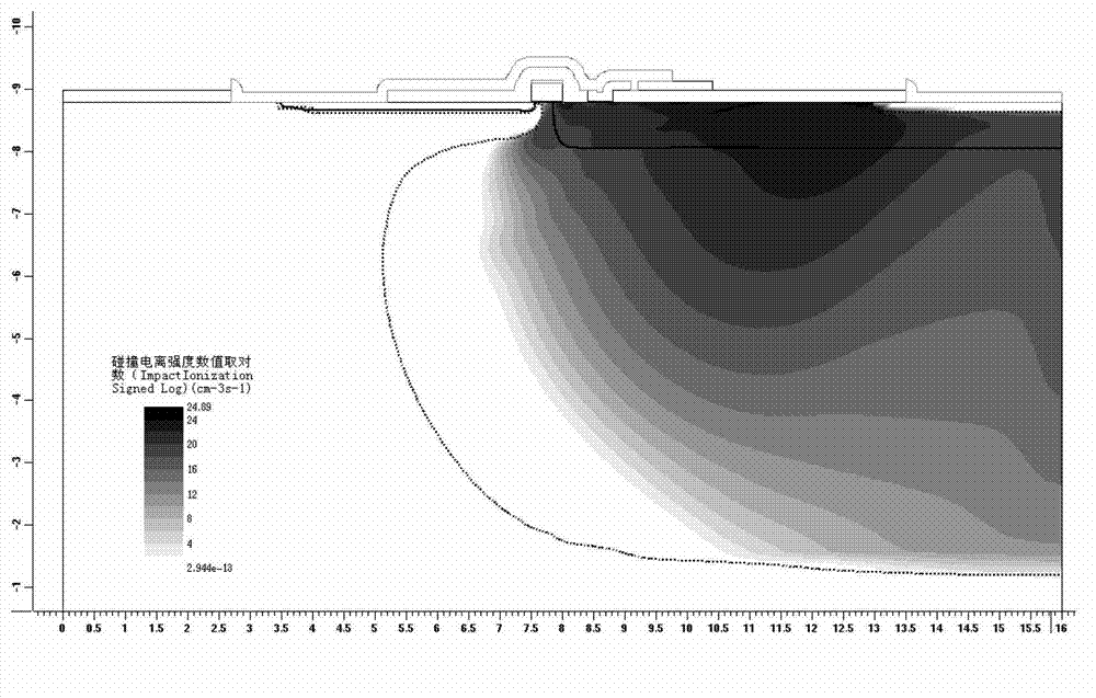
[0053] like figure 2 As shown, it is the structure of the RFLDMOS device of the present invention, which includes growing a P-type epitaxial layer 22 with different thicknesses and doping concentrations on the P-type substrate 21; then growing a gate oxide layer 24 by thermal oxygen; depositing Polysilicon, the lithography board defines and etched the polysilicon gate 25; ion implantation is performed to form a lightly doped drift region (NLDD) 23; ion implantation and diffusion processes are used to form P well 26, P+ region 27, N+ source region 28 and N+ drain respectively Region 29; a silicon oxide layer 210 is deposited over the P-type epitaxial layer 22 as a whole, a silicon nitride layer 211 is arranged on the silicon oxide l...


PUM

PropertyMeasurementUnit
Thicknessaaaaaaaaaa
Lengthaaaaaaaaaa
Thicknessaaaaaaaaaa

Abstract

The invention discloses a field effect transistor of a radio frequency lateral double-diffusion which comprises a P-type substrate. A P-type epitaxial layer is formed on the P-type substrate in an epitaxial growth mode, and a veneer of monox layer is deposited on the upper portion of the P-type epitaxial layer. A veneer of metal layer is deposited on the monox layer and formed a faraday layer in an etching form. A veneer of silicon nitride layer is arranged between the monox layer and the faraday layer. The field effect transistor of the radio frequency lateral double-diffusion has the advantages of reducing one metal deposition process, meanwhile achieving higher breakdown voltage (BV), reducing the electric field intensity of the lower portion of gate-oxide edge, and helping to restrain domino effect of (HCI) hot carrier injection.

Description

technical field [0001] The invention relates to a semiconductor integrated circuit manufacturing device, in particular to a radio frequency lateral double-diffusion field effect transistor, and the invention also relates to a manufacturing method of the transistor. Background technique [0002] The RF Lateral Double Diffusion Field Effect Transistor (RFLDMOS) device is a new generation of integrated solid-state microwave power semiconductor products formed by the fusion of semiconductor integrated circuit technology and microwave electronic technology. It has good linearity, high gain, high withstand voltage and high output power. , good thermal stability, high efficiency, good broadband matching performance, easy to integrate with MOS process, and its price is much lower than gallium arsenide devices, is a very competitive power device, is widely used in GSM, PCS, power amplifiers of W-CDMA base stations, as well as wireless broadcasting and nuclear magnetic resonance. [...

Claims


Application Information

Patent Timeline
IPC IPC(8): H01L21/336H01L29/78H01L23/60
CPCH01L29/7835H01L29/1045H01L29/402H01L29/404
Inventor 李娟娟慈朋亮钱文生韩峰胡君
Owner SHANGHAI HUAHONG GRACE SEMICON MFG CORP
Why Eureka
Try Eureka