rfldmos device and manufacturing method

A manufacturing method and device technology, applied in semiconductor/solid-state device manufacturing, semiconductor devices, electrical components, etc., can solve problems such as large base resistance, device voltage failure, snapback effect, etc., to reduce base resistance, The effect of improving transconductance and reducing hot carrier effect

Active Publication Date: 2015-08-19
SHANGHAI HUAHONG GRACE SEMICON MFG CORP
View PDF5 Cites 0 Cited by
  • Summary
  • Abstract
  • Description
  • Claims
  • Application Information

AI Technical Summary

Problems solved by technology

The metal can reduce the resistance of the substrate and improve the thermal diffusion ability, but the device with this structure still has the base resistance R B Larger, there may be a snapback effect, causing the tube to burn and other device voltage resistance failures to occur

Method used


Image

  • rfldmos device and manufacturing method
  • rfldmos device and manufacturing method
  • rfldmos device and manufacturing method

Examples


Embodiment Construction

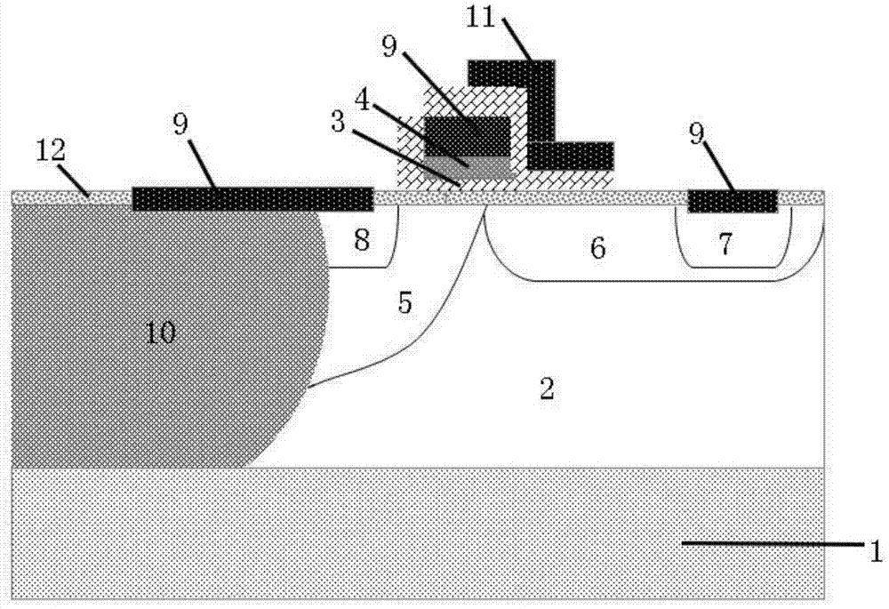
[0037] The structure of RFLDMOS device described in the present invention is as Figure 14 Shown:

[0038] On the P-type silicon substrate 311 , there is a lightly doped P-type epitaxy 312 .

[0039] In the lightly doped P-type epitaxy 312 , there is an N-type lightly doped drain drift region 317 and a P-type channel region 316 abutting against it.

[0040] The N-type lightly doped drain drift region 317 includes the drain region 321 of the RFLDMOS device, and the surface of the drain region 321 has a metal silicide 319 leading to the drain of the RFLDMOS device.

[0041] The P-type channel region 316 includes a heavily doped P-type channel connection region 322 and a heavily doped N-type region 320 abutting against it. The heavily doped N-type region 320 is the RFLDMOS device. source area.

[0042] The surface of the heavily doped P-type channel connection region 322 and the source region 320 of the RFLDMOS is covered with a layer of metal silicide 319 leading to the sourc...


PUM


Abstract

A radio frequency (RF) laterally diffused metal oxide semiconductor (LDMOS) device is disclosed which additionally includes a lightly-doped P-type buried layer under a P-type channel region and a moderately-dope P-type buried layer in the lightly-doped P-type buried layer. The two buried layers result in a lower base resistance for an equivalent parasitic NPN transistor, thereby impeding the occurrence of snapback in the device. Additionally, an equivalent reverse-biased diode formed between the channel region and the buried layers is capable of clamping the drain-source voltage of the device and sinking redundant currents to a substrate thereof. Furthermore, the design of a gate oxide layer of the RF LDMOS device to have a greater thickness at a proximal end to a drain region can help to reduce the hot-carrier effect, and having a smaller thickness at a proximal end to the source region can improve the transconductance of the RF LDMOS device.

Description

technical field [0001] The invention relates to the field of semiconductor integrated circuits, in particular to an RFLDMOS applied to high-power radio frequency signal amplification. The present invention also relates to a manufacturing method of said RFLDMOS device. Background technique [0002] RFLDMOS (Radio Frequency Laterally Diffused Metal Oxide Semiconductor) is a semiconductor with high gain, high linearity, high withstand voltage, and high output power, which is widely used in radio and television transmitting base stations, mobile transmitting base stations, radars, etc. RF power devices have two operating voltages of 28V and 50V, and the corresponding breakdown voltage requirements are 70V and 120V respectively. The basic structure of the device is as figure 1 As shown, it is an N-type device, and the higher withstand voltage is determined by the length of the N-type low-doped drift region 6 (the distance from the heavily doped N-type drain terminal 7 to the ed...

Claims


Application Information

Patent Timeline
Patent Type & Authority Patents(China)
IPC IPC(8): H01L29/78H01L29/10H01L29/08H01L21/336
CPCH01L29/7823H01L29/66681H01L29/402H01L29/42368H01L29/423H01L29/66659H01L29/7835H01L29/1083
Inventor 周正良遇寒蔡莹陈曦
Owner SHANGHAI HUAHONG GRACE SEMICON MFG CORP
Why Eureka
Try Eureka