VDMOS transistor and preparation method thereof

A technology of transistors and polysilicon layers, applied in semiconductor/solid-state device manufacturing, semiconductor devices, electrical components, etc., can solve problems such as poor reliability, VDMOS performance degradation, and increased gate leakage current, achieving small leakage current, Good reliability and less number of steps

Inactive Publication Date: 2013-04-10
SOUTH CHINA UNIV OF TECH
View PDF6 Cites 21 Cited by
  • Summary
  • Abstract
  • Description
  • Claims
  • Application Information

AI Technical Summary

Problems solved by technology

[0007] The existing technology has not clearly aimed at overcoming the significant increase in gate leakage current cau

Method used


Image

  • VDMOS transistor and preparation method thereof
  • VDMOS transistor and preparation method thereof
  • VDMOS transistor and preparation method thereof

Examples


Embodiment 1

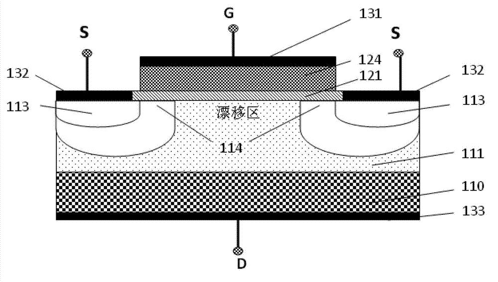
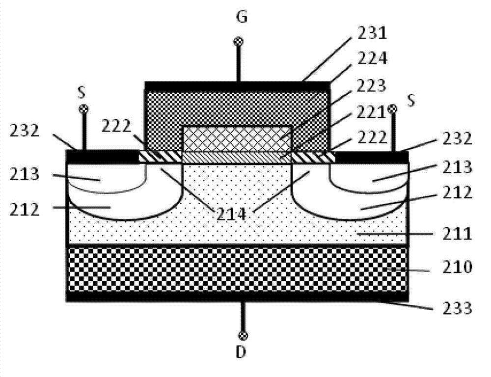
[0075] The first conductivity type is N-type, the second conductivity type is P-type, the prepared transistor is an N-channel MOS transistor, and the provided substrate is a silicon substrate.

[0076] A kind of preparation method of VDMOS transistor, comprises, in N + Fabrication of N over silicon substrates - epitaxial layer, the N - A gate structure is fabricated over the epitaxial layer.

[0077] The preparation method of the gate structure specifically includes the following steps:

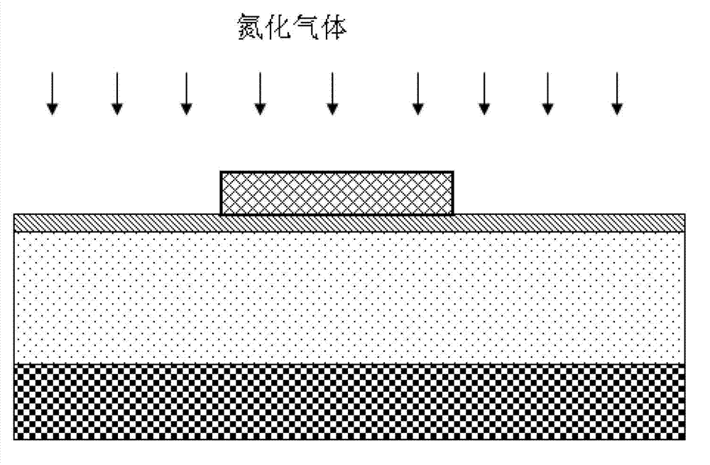
[0078] (1) A thermal oxidation method is used to form a thickness of the silicon dioxide layer;

[0079] (2) On the surface of the silicon dioxide layer, a semi-insulating polysilicon SIPOS layer is formed by a low-pressure chemical vapor deposition method, and a silane SiH 4 and laughing gas N 2 O is used as the reaction gas, and by controlling the flow ratio of the reaction gas and other process conditions, the thickness of the semi-insulating polysilicon SIPOS is about Resistivity...


PUM

PropertyMeasurementUnit
Resistivityaaaaaaaaaa

Abstract

The invention discloses a VDMOS transistor and a preparation method thereof and belongs to the field of semiconductors. The VDMOS transistor comprises a first conduction type substrate, a first conduction type epitaxial layer, a second conduction type injection region, a first conduction type highly doped source region and a grid structure, the second conduction type injection region and the first conduction type highly doped source region are arranged in the epitaxial layer, and the grid structure comprises a grid insulating layer, a semi-insulating polycrystalline silicon layer, a silicon oxynitride layer and a polycrystalline silicon layer. The grid insulating layer is arranged above a drift region of the epitaxial layer, the semi-insulating polycrystalline silicon layer is arranged above the grid insulating layer, the silicon oxynitride layer is arranged above a channel region, and the polycrystalline silicon layer is covered on the semi-insulating polycrystalline silicon layer and the silicon oxynitride layer. A heat nitriding silicon oxynitride layer is introduced into the preparation method, a traditional silica layer which is used as a gate medium layer on a channel is replaced, and the semi-insulating polycrystalline silicon layer is added on an oxide layer which is arranged above the drift region of the epitaxial layer. The VDMOS transistor and the preparation method thereof can obviously reduce grid-drain capacitance and achieve overcoming the defects that insulating performance of the grid insulating layer is poor, current leaking of a grid electrode is increased, and degeneration of the VDMOS performance is unreliable.

Description

technical field [0001] The invention relates to the field of semiconductor devices, in particular to a VDMOS transistor and a preparation method thereof. Background technique [0002] Vertical conductive double-diffused field effect transistor (VDMOSFET, hereinafter referred to as VDMOS) is a semiconductor power device with high input impedance, high thermal stability, fast switching speed, small driving current, small dynamic loss, and small distortion. , industrial control, automotive electrical appliances and other fields have been widely used. [0003] figure 1 It is a schematic diagram of a cross-sectional structure of a traditional N-channel VDMOS transistor. Such as figure 1 As shown, taking the N-channel MOS transistor as an example, the vertical double-diffused MOS transistor is in the highly doped N + A layer of low-doped N - The doping level of the epitaxial layer 111 and the epitaxial region largely determines the breakdown voltage of the device. There is a...

Claims


Application Information

Patent Timeline
IPC IPC(8): H01L29/78H01L29/51H01L21/336H01L21/285
Inventor 郑学仁
Owner SOUTH CHINA UNIV OF TECH
Why Eureka
Try Eureka