Package substrate and its manufacturing method and LED package structure based on the package substrate

A technology for LED packaging and packaging substrates, applied in electrical components, electrical solid devices, circuits, etc., can solve the problems of complex manufacturing process, rising PN junction junction temperature, aging of chips and packaging materials, etc., to simplify the manufacturing process, Reduced production cost and increased installation height

Active Publication Date: 2015-09-09
ELEC TECH OPTOELECTRONICS TECHWUHUCO
View PDF6 Cites 0 Cited by
  • Summary
  • Abstract
  • Description
  • Claims
  • Application Information

AI Technical Summary

Problems solved by technology

[0003] Although LED is energy-saving, but like ordinary incandescent lighting, part of the energy is converted into light, and another part of the energy is converted into heat, especially LED is a point-shaped light source, and the heat generated by it is also concentrated in a very small area. The heat generated cannot be dissipated in time, and the junction temperature of the PN junction will rise, which will accelerate the aging of the chip and packaging materials, and may also cause the solder joints to melt, causing the chip to fail, which will directly affect the service life and luminous performance of the LED, especially High-power LEDs generate more heat and require higher heat dissipation technology
[0004] Ceramic substrates have the advantages of high heat dissipation, low thermal resistance, long life, wide operating temperature, and withstand voltage. However, the preparation of ceramic heat dissipation substrates requires high equipment and technology, and the manufacturing process is quite complicated. , evaporation, sputtering, electroplating, and electroless plating make the ceramic substrate expensive
In addition, in the traditional ceramic substrate, the bonding glue of the packaging lens and the copper-metal composite layer will have a certain impact on the light output of the LED chip. This part of the glue blocks a part of the light emitted from the side of the LED chip, making the use of LED side light rate drop
For this problem, technical personnel in the industry have also proposed improvements, such as the Chinese patent No. 201220168404.8, which discloses a substrate structure for LED chip packaging, although this solution solves the problem of using traditional ceramic substrates to reduce the lateral light output rate of LED chips. problem, but the design of the circuit layer and the micron-scale ultra-thin ceramic insulating layer increases the complexity of the process. In addition, the patent uses a tungsten-copper alloy panel with bosses, which increases the cost of materials, making this packaging substrate The costly problem remains unresolved

Method used


Image

  • Package substrate and its manufacturing method and LED package structure based on the package substrate
  • Package substrate and its manufacturing method and LED package structure based on the package substrate
  • Package substrate and its manufacturing method and LED package structure based on the package substrate

Examples


Embodiment Construction

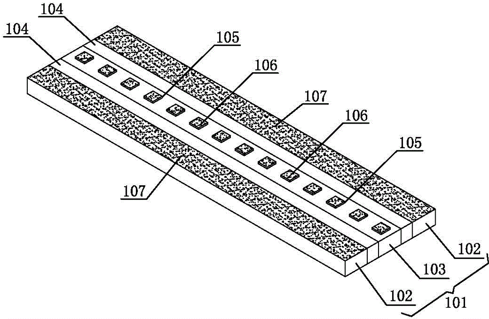
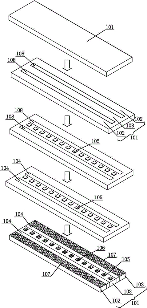
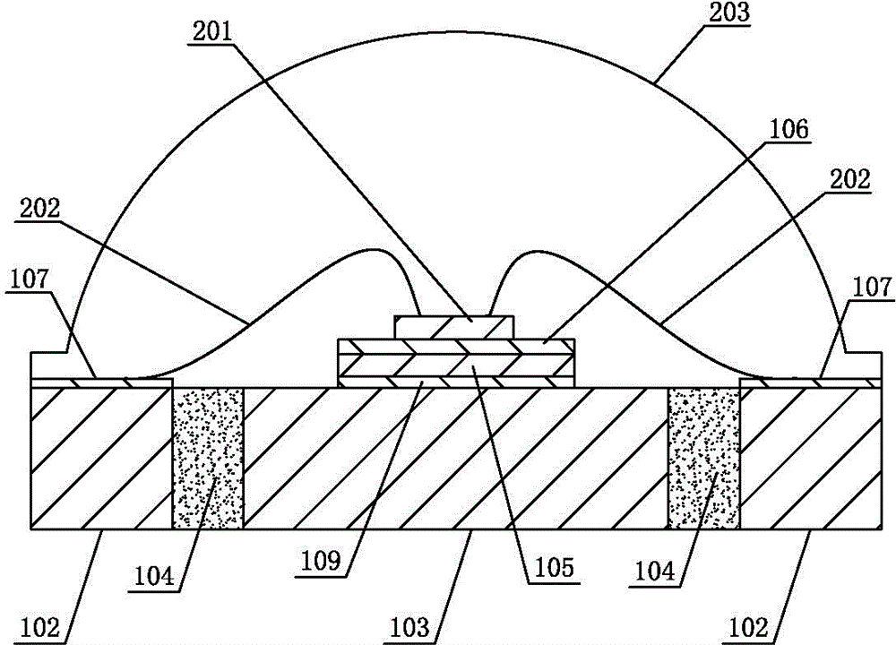
[0028] see figure 1 , the package substrate shown in the figure includes: a copper heat sink plate 101, two insulating strips 104 are embedded on the copper heat sink plate 101, and the two insulating strips 104 separate the copper heat sink plate 101 into Electrode 102, welding strip 103, three regions of electrode 102, welding strip 103 is positioned between two electrodes 102; The tungsten-copper alloy boss 105 that fixes LED chip passes silver-copper solder layer (see image 3 ) are welded on the welding strip 103, and electroplating layers 106 and 107 are respectively provided on the surfaces of the tungsten-copper alloy boss 105 and the two electrodes 102. Preferably, the electroplating layers 106 and 107 are provided with two layers of nickel electroplating layer (not shown) and silver electroplating layer (not shown in the figure) from the inside to the outside, and the silver electroplating layer covers the nickel electroplating layer; or, the nickel electroplating la...


PUM


Abstract

The invention provides a package substrate which comprises a copper heat sink plate. Two insulating belts are inlaid on the copper heat sink plate, and the copper heat sink plate is divided into three areas, respectively an electrode area, a welding belt area and an electrode area by the two insulating belts. Tungsten-copper alloy bosses used for fixing light-emitting diode (LED) chips are welded on the welding belt area, and electroplated layers are respectively arranged on the tungsten-copper alloy bosses and the surfaces of the two electrodes. The package substrate is simple in structure, capable of simplifying manufacturing process of the package substrate and greatly reducing manufacturing cost of an LED package substrate. Installation height of the LED chip in a lamp is increased by the tungsten-copper alloy bosses, and therefore light emitted by the LED chips can directly light on working faces of package lenses. The problem that a light extracting rate can be influenced by bonding glue of lenses of a traditional ceramic substrate is solved, and a light emitting rate of an LED bead is increased.

Description

technical field [0001] The invention relates to the technical field of LED packaging, in particular to a packaging substrate, a manufacturing method thereof, and an LED packaging structure based on the packaging substrate. Background technique [0002] LED (Light Emitting Diode) is a solid-state semiconductor device that converts electrical energy into light energy. With the advantages of low power consumption, good light concentrating effect, fast response, strong controllability, high impact resistance, long service life, and environmental protection, LED is gradually replacing traditional light sources and becoming the fourth-generation light source. [0003] Although LED is energy-saving, but like ordinary incandescent lighting, part of the energy is converted into light, and another part of the energy is converted into heat, especially LED is a point-shaped light source, and the heat generated by it is also concentrated in a very small area. The heat generated cannot b...

Claims


Application Information

Patent Timeline
Patent Type & Authority Patents(China)
IPC IPC(8): H01L33/48H01L33/62H01L33/64
CPCH01L2224/48091H01L2224/73265H01L2924/181
Inventor 王冬雷武文成庄灿阳
Owner ELEC TECH OPTOELECTRONICS TECHWUHUCO
Why Eureka
Try Eureka