Method for performing solderability treatment on the surface of welding area while making solder resist pattern

A welding area and solderability technology, which is applied in the secondary treatment of printed circuits, coating of non-metallic protective layers, etc., can solve the requirements of more refined packaging structure of electronic components and the difficulty of welding fine-pitch components , not suitable for fine-pitch circuit boards, etc., to achieve the effect of reducing environmental burden, small site, and improving accuracy

Active Publication Date: 2015-09-23
德中(天津)技术发展股份有限公司
View PDF3 Cites 0 Cited by
  • Summary
  • Abstract
  • Description
  • Claims
  • Application Information

AI Technical Summary

Problems solved by technology

[0004] Coating solder resist usually adopts screen printing method and photochemical imaging method. No matter which method is used, it is first necessary to draw the base plate first, then transfer the pattern, and then directly screen print to form a solder resist pattern or coat the whole board with liquid photoresist Soldering paint, after pre-drying, exposure, and development, forms a solder resist pattern. The disadvantages are: the two methods require a long process route, and due to the limitation of graphic resolution, it is difficult to adapt to the requirements of more refined packaging structures of electronic components. It is one of the reasons for the difficulty in soldering fine pitch components
This hot air leveling method has certain limitations. SMT technology has higher requirements on circuit boards. In addition to problems such as plugging holes and bridging, the circuit board is subjected to thermal shock when it is immersed in solder, which may cause deformation of the circuit board. During the lifting process from the solder tank, the gravity and surface tension of the solder itself make the solder on the surface of the pad thinner at the top and thicker at the bottom, and uneven, all of which are the source of soldering defects
On the other hand, the use of lead-containing solder is not suitable for lead-free processes, and the burden on the environment is large
Hot air leveling technology is not suitable for SMT with pitch less than 0.5mm
In addition, hot air leveling needs to work at high temperature, and the equipment needs stainless steel, titanium or other alloys. The investment in equipment is large, the process is complicated, and the operating environment is harsh. It is not suitable for fine-pitch circuit boards.

Method used


Image

  • Method for performing solderability treatment on the surface of welding area while making solder resist pattern
  • Method for performing solderability treatment on the surface of welding area while making solder resist pattern
  • Method for performing solderability treatment on the surface of welding area while making solder resist pattern

Examples


Embodiment 1

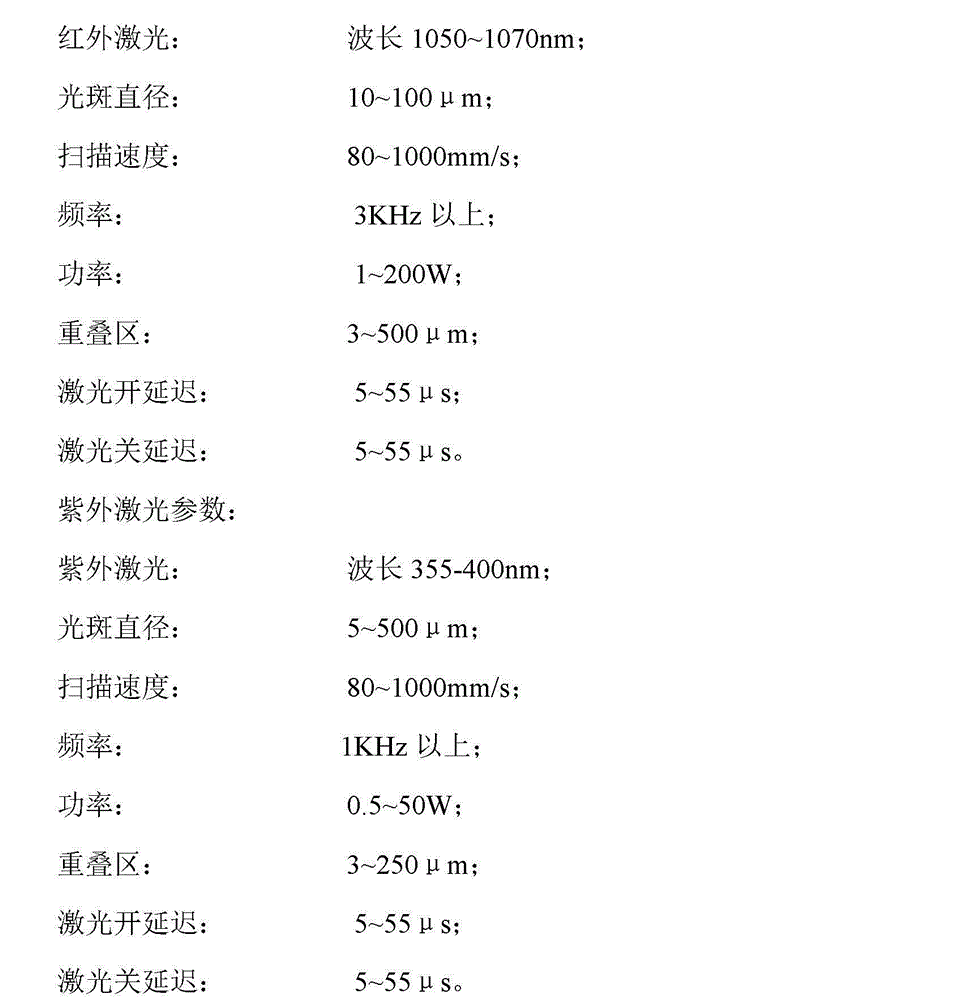
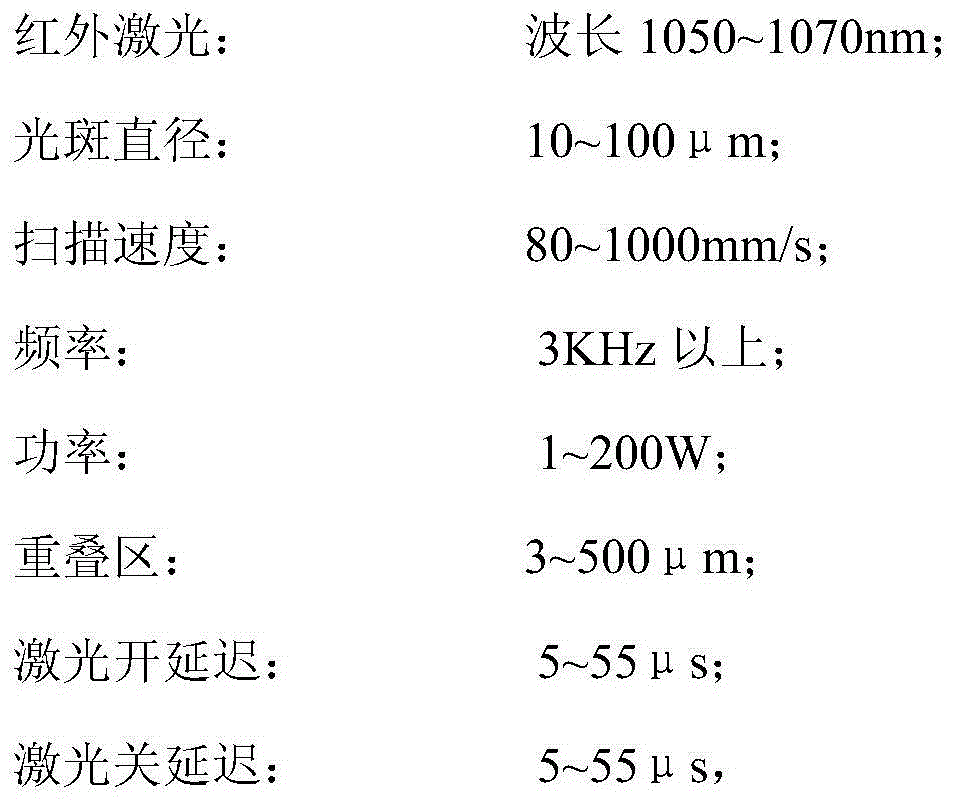
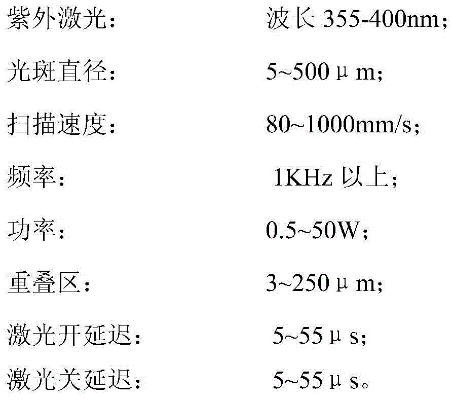
[0038] A method for performing solderability treatment on the surface of a welding zone while making a solder resist pattern, the steps of which are:

[0039] (1) Solder resist coating: Coat the entire board by screen printing, use 43T mesh to coat the photosensitive ink C-7 on the board, and let it stand for 10~20min after missing printing;

[0040] ⑵Solder resist curing: Put the plate after standing still in the drying oven to bake, and cure the photosensitive ink C-7 in two stages, after curing for 30 minutes at 75±2°C, and then curing for 70 minutes at 150°C;

[0041] (3) Data import: Import the data of the solder mask layer, process it with data processing software, obtain the laser processing path, and import the processing path into the laser equipment control software;

[0042] ⑷Laser photoetching: place the cured photosensitive ink C-7 on the laser equipment, and accurately align the top layer of the board with the processing path, and perform photoetching on the top ...

Embodiment 2

[0047] A method for performing solderability treatment on the surface of a welding zone while making a solder resist pattern, the steps of which are:

[0048] (1) Solder resist coating: Coat the entire board by screen printing, use 43T mesh to coat the photosensitive ink UPC-9000 on the board, and let it stand for 10~20 minutes after missing printing;

[0049] ⑵Solder resist curing: Put the plate after standing still in the drying oven to bake, and cure the photosensitive ink UPC-9000 in two stages, after curing for 50 minutes at 67±2°C, and then curing for 60 minutes at 150°C;

[0050] (3) Data import: Import the data of the solder mask layer, process it with data processing software, obtain the laser processing path, and import the processing path into the laser equipment control software;

[0051] ⑷Laser photoetching: Place the in-process panel after the photosensitive ink UPC-9000 is cured on the laser equipment, accurately align the top layer of the in-process panel with ...

Embodiment 3

[0056] A method for performing solderability treatment on the surface of a welding zone while making a solder resist pattern, the steps of which are:

[0057] (1) Solder resist coating: Coat the entire board by screen printing, use 43T mesh to coat the photosensitive ink VSR-ZG on the board, and let it stand for 10~20min after missing printing;

[0058] ⑵Solder resist curing: put the board after standing still into the UV curing equipment to cure the photosensitive ink VSR-ZG, the light energy density is 12μW / cm2, and the transmission speed of the board is 1.5-2.0m / min;

[0059] (3) Data import: Import the data of the solder mask layer, process it with data processing software, obtain the laser processing path, and import the processing path into the laser equipment control software;

[0060] ⑷Laser photoetching: place the cured photosensitive ink VSR-ZG on the laser equipment, align the top layer of the board with the processing path accurately, and perform photoetching on th...


PUM


Abstract

The invention relates to a method for producing a resistance soldering pattern and capable of conducting solderability treatment on a surface of a welding area, and the method comprises the following steps of coating solder resist on an entire circuit board bare board, solidifying the solder resist on the entire board, producing a resistance soldering pattern through laser photoetching, conducting surface treatment on the welding area of the circuit board bare board, and obtaining a printed circuit board with good surface soldability. The production of the resistance soldering pattern and the surface treatment of the welding area are sequentially completed on a laser device, so that the production flow is simplified, the coating process of a solderable protection material and relevant devices can be saved, the material is greatly saved, the energy consumption is reduced, the investment expenditure and the production cost are reduced, the environmental load is alleviated, the inhalation of operators on harmful substances can be avoided, the production flow is shorted, the needed investment is low, and the needed field is small.

Description

technical field [0001] The invention belongs to the field of printed circuit boards, and relates to surface solderability treatment of printed circuit boards, in particular to a method for performing solderability treatment on the surface of a welding area while making a solder resist pattern. Background technique [0002] The manufacturing process of circuit boards usually includes two production stages: bare board manufacturing and circuit board assembly. Among them, the bare board refers to the circuit board that has not yet installed components, also known as printed circuit board, printed circuit board, printed circuit board, circuit board. The above-mentioned bare boards are generally customized in the circuit board manufacturing plant. Usually, this kind of bare board customized in the circuit board manufacturing plant is called the board in process. Taking double-sided circuit boards as an example, the process flow is roughly: cutting - drilling And hole metallizati...

Claims


Application Information

Patent Timeline
Patent Type & Authority Patents(China)
IPC IPC(8): H05K3/28
Inventor 胡宏宇于跃欣屈元鹏郑国平
Owner 德中(天津)技术发展股份有限公司
Why Eureka
Try Eureka