

Method for preparing array substrate for liquid crystal display device
A technology for liquid crystal display devices and array substrates, applied in chemical instruments and methods, optics, instruments, etc., can solve problems such as difficult to use grid lines and data lines, and achieve the effects of preventing electrical short circuits and being environmentally friendly
Active Publication Date: 2013-04-17
DONGWOO FINE CHEM CO LTD
View PDF5 Cites 27 Cited by
- Summary
- Abstract
- Description
- Claims
- Application Information
AI Technical Summary
Problems solved by technology
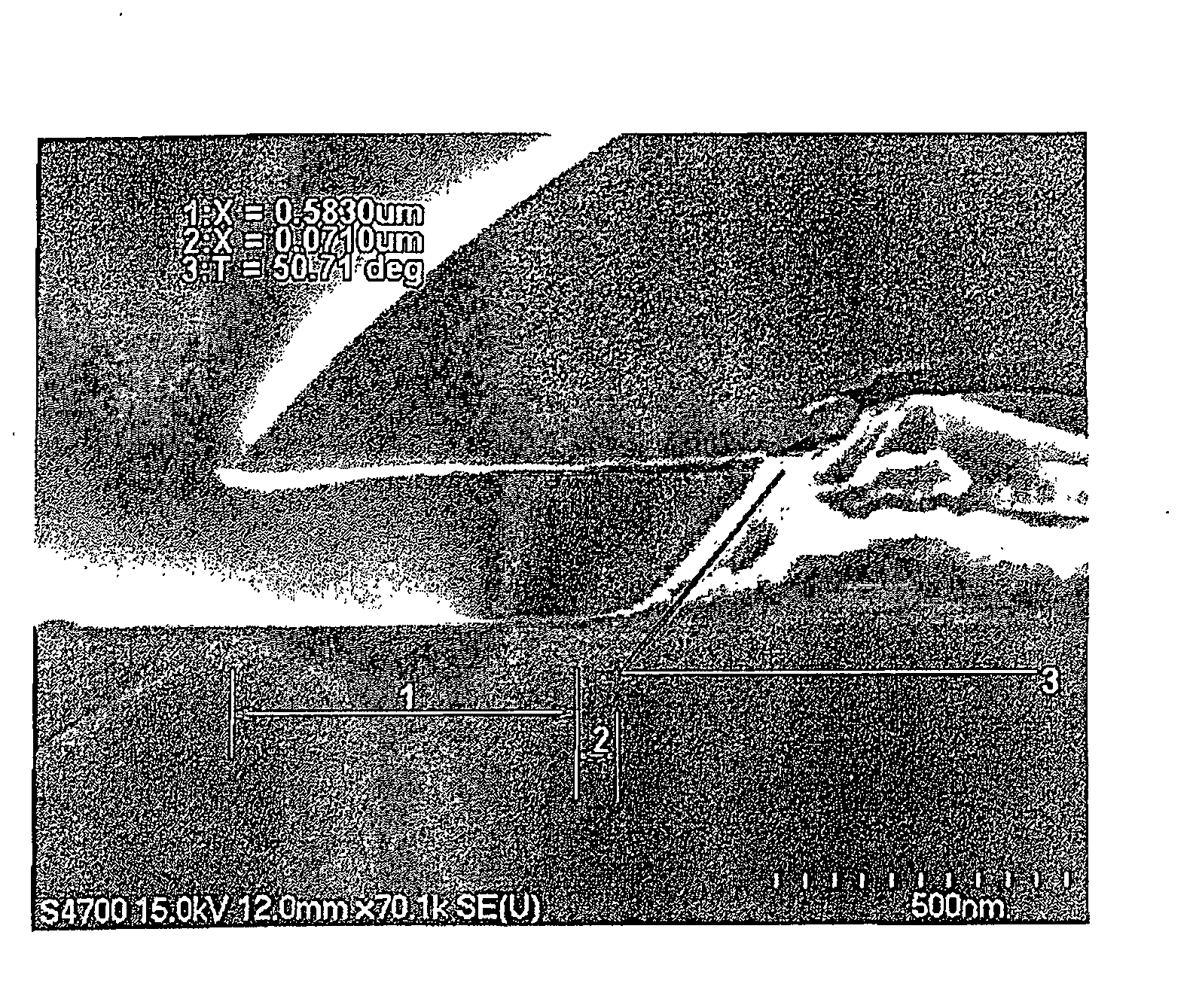
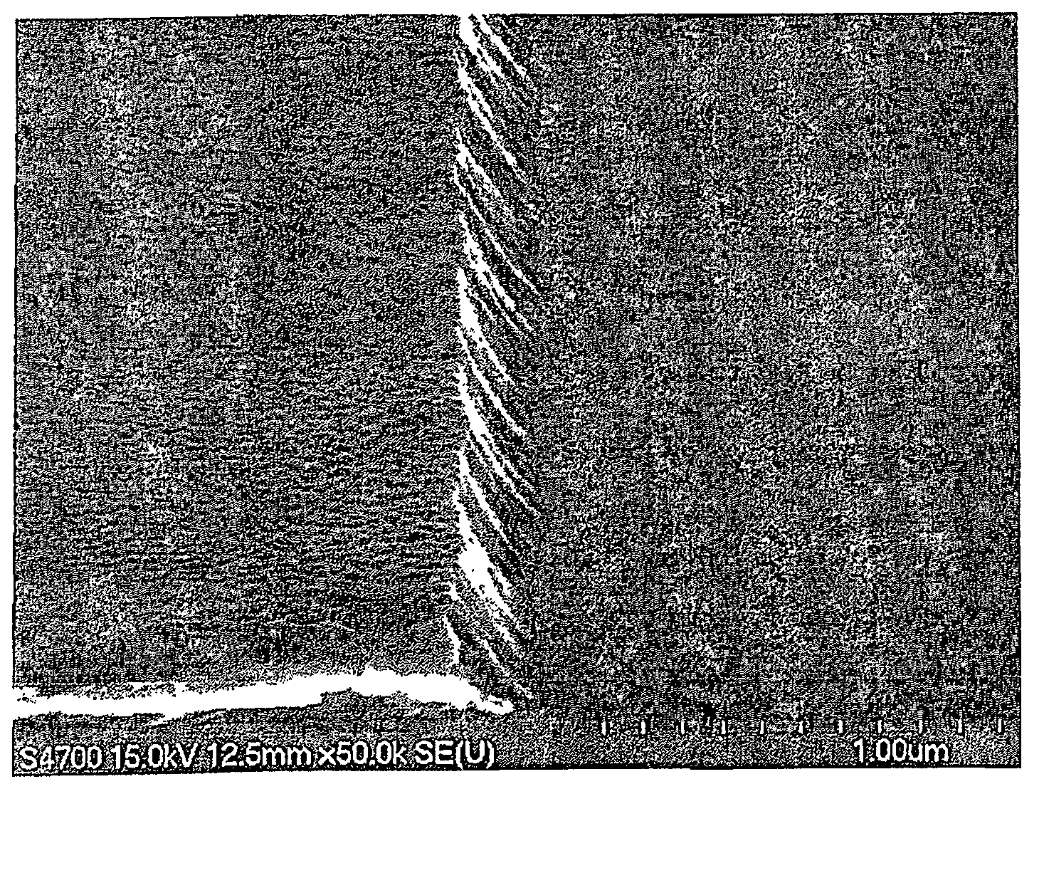
Traditionally, chromium (Cr, resistivity: 12.7×10 -8 Ωm), molybdenum (Mo, resistivity: 5×10 -8 Ωm), aluminum (Al, resistivity: 2.65×10 -8 Ωm), and their alloys, but in fact it is difficult to use for large TFT-LCD gate lines and data lines
Method used
View moreImage
Smart ImageViewing Examples

Examples
Embodiment 1 to 6
[0052] Embodiments 1 to 6: Preparation of etchant composition for Cu-based metal layer
[0053] Etchant compositions of Examples 1 to 6 were prepared according to the ingredients shown in Table 1 below.
[0054] Table 1
[0055]
Login to View More PUM
| Property | Measurement | Unit |
|---|---|---|
| electrical resistivity | aaaaa | aaaaa |
Abstract
The present invention relates to preparation method for an array substrate for the use in a liquid crystal display device, using an etchant composition comprising: a) 5-25 wt% of hydrogen peroxide (H2O2); b) 0.1-5 wt% of an organic acid; c) 0.1-5 wt% of a phosphate compound; d) 0.1-5 wt% of a water-soluble cyclic amine compound; e) 0.1-5 wt% of a water-soluble compound having a nitrogen atom and a carboxyl group in a molecule; f) 0.01-1.0 wt% of a fluorine-containing compound; g) 0.001-5 wt% of a polyhydric alcohol-based surfactant; and h) the balance of water based on the total weight of the composition.
Description
technical field [0001] The invention relates to a method for manufacturing an array substrate for a liquid crystal display device. Background technique [0002] Forming metal wiring on a substrate of a semiconductor device includes forming a metal layer, coating a photoresist, exposing and developing to form a photoresist on a selective area, and performing etching. In addition, forming metal wiring includes cleaning procedures before and after each individual process. The etching process is performed using a photoresist as a mask so that a metal layer is formed on a selective area, and generally includes dry etching using plasma, or wet etching using an etchant composition. [0003] In this semiconductor device, the resistance of metal wiring has recently been regarded as important. This is because resistance is the dominant factor in inducing RC signal delay. In particular, in the case of a thin film transistor-liquid crystal display device (TFT-LCD), related technologi...
Claims
Login to View More Application Information
Patent Timeline
 Patent Type & AuthorityApplications(China)
IPC IPC(8): G02F1/136C09K13/08
CPCH01L29/4908H01L27/124H01L27/1259
Inventor崔容硕李石尹暎晋李友兰
OwnerDONGWOO FINE CHEM CO LTD