A wafer-level through-silicon transmission structure applicable to microwave frequency bands and its manufacturing method

A technology of microwave frequency band and transmission structure, applied in semiconductor/solid-state device manufacturing, waveguide, waveguide-type devices, etc., can solve the problems of lithography capability and lithography precision limitation, coaxial line difficulties, etc., and achieve small mechanical and physical damage , Guaranteed precision and simple process steps

Inactive Publication Date: 2015-07-29
SHANGHAI INST OF MICROSYSTEM & INFORMATION TECH CHINESE ACAD OF SCI
View PDF2 Cites 0 Cited by
  • Summary
  • Abstract
  • Description
  • Claims
  • Application Information

AI Technical Summary

Problems solved by technology

However, this method is limited by the lithographic ability and lithographic accuracy of thick film materials, and it is difficult to prepare coaxial lines with high aspect ratios.

Method used


Image

  • A wafer-level through-silicon transmission structure applicable to microwave frequency bands and its manufacturing method
  • A wafer-level through-silicon transmission structure applicable to microwave frequency bands and its manufacturing method
  • A wafer-level through-silicon transmission structure applicable to microwave frequency bands and its manufacturing method

Examples


Embodiment 1

[0027] exist Figure 2-1-Figure 2-10 In , the process flow of the wafer-level through-silicon transmission structure applied in the microwave frequency band is introduced in detail.

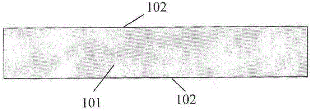
[0028] 1. Surface pretreatment of silicon wafer 101, growth of oxide layer 102, such as diagram 2-1 shown.

[0029] a) performing surface pretreatment on both sides of the silicon wafer 101;

[0030] b) growing an oxide layer 102 as a mask.

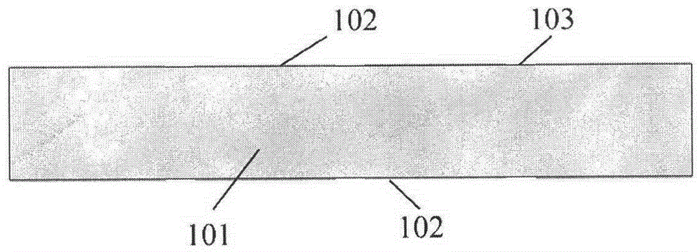
[0031] 2. Form the through hole etching window 103, such as Figure 2-2 shown.

[0032] a) Forming a through-hole etching window 103 on the front surface of the silicon wafer 101 by photolithography, development and etching.

[0033] 3. Form blind holes (holes that are not pierced) 104, such as Figure 2-3 shown.

[0034] a) Form a vertical silicon blind hole 104 with a depth of half the thickness of the silicon wafer (for example, about 225 μm) on the front surface of the silicon wafer 101 by deep reactive ion etching (DRIE) process.

[0035] 4. Fo...


PUM


Abstract

The present invention relates to a wafer-level through-silicon via (TSV) transmission structure applicable to the microwave band and a manufacturing method thereof. A TSV transmission cable structure using a high-frequency alternative coaxial cable structure is designed. In the structure, multiple TSVs surround a TSV core for signal transmission. The surrounding TSVs are grounded. A coaxial shielding layer similar to that of the coaxial cable is formed. Two opposite sides of the silicon piece between the grounded TSV and the TSV chip each use an isolation groove filled with low dielectric constant polymer. The number, size, and distance of the grounded via holes are determined through simulation of an actually applied frequency band. The structure realizes interconnection of the two sides of the silicon piece of the microwave band. The TSV transmission structure reduces the impact on the microwave band performance when a signal passes through a silicon piece in high-density three-dimensional package, and avoids excessive loss. The process has simple steps, and is compatible with other processes.

Description

technical field [0001] The invention relates to a wafer-level through-silicon transmission structure and a manufacturing method that can be used in microwave frequency bands, and belongs to the field of high-density packaging. Background technique [0002] People's demand for more functions, higher performance, smaller volume and lower cost of electronic devices has prompted the vigorous development of various three-dimensional integration and related packaging technologies, such as MCM (multi-chip components), SiP (system-in-package), CSP (Chip Scale Package), WLP (Wafer Level Package), etc. The current mainstream chip manufacturing and integration technology is to process one side of the wafer and make a corresponding protective layer on the other side of the chip. If both sides of the wafer can be utilized, the integration and packaging density will be greatly improved. Through-silicon via technology has become one of the most promising technologies because of its high-...

Claims


Application Information

Patent Timeline
Patent Type & Authority Patents(China)
IPC IPC(8): H01L23/48H01L21/768
CPCH01P3/06H01L2924/0002H01L23/66H01P11/005H01L2924/10253H01L21/76898H01L2223/6622H01L23/481H01L2924/00
Inventor 汤佳杰罗乐丁晓云徐高卫陈骁
Owner SHANGHAI INST OF MICROSYSTEM & INFORMATION TECH CHINESE ACAD OF SCI
Why Eureka
Try Eureka