AAQFN package part using electroplating process and manufacture process thereof

An electroplating process and manufacturing process technology, which is applied in the manufacture of electrical components, electrical solid devices, semiconductor/solid devices, etc., can solve the problems of cumbersome packaging process and increased packaging costs, so as to improve electrical performance and product reliability, save Package cost, wear prevention effect

Inactive Publication Date: 2013-05-08
HUATIAN TECH XIAN
View PDF4 Cites 7 Cited by
  • Summary
  • Abstract
  • Description
  • Claims
  • Application Information

AI Technical Summary

Problems solved by technology

[0005] However, the traditional AAQFN packaging process mainly uses stencil brushing solder paste, and then reflows the solder paste, which not only increases the packaging cost to a certain extent, but also cumbersome packaging process

Method used


Image

  • AAQFN package part using electroplating process and manufacture process thereof
  • AAQFN package part using electroplating process and manufacture process thereof
  • AAQFN package part using electroplating process and manufacture process thereof

Examples


Embodiment Construction

[0021] The present invention will be described in further detail below in conjunction with the accompanying drawings.

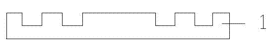
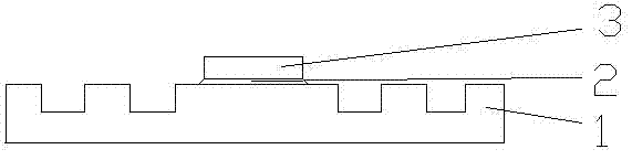
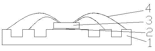
[0022] As shown in the figure, an AAQFN package using an electroplating process is mainly composed of a copper lead frame 1, a die adhesive 2, a chip 3, a bonding wire 4, a molding compound 5, a solder resist layer 6 and a solder ball 7. The copper lead frame 1 is first half-etched, and then the chip 3 and the etched copper lead frame 1 are bonded with the adhesive 2, and the chip 3 and the etched copper frame 1 pin are bonded. The connecting wire 4 is connected, and then plastic-sealed with a plastic encapsulant 5. The copper pin 1 is to etch the bottom of the half-etched copper frame to separate the pins, and then fill the etched pins at the bottom with a solder resist layer 6 The voids are then electroplated with tin balls 7 using an electroplating process, followed by product cutting.

[0023] As shown in the figure, a manufacturing process of an AAQFN p...


PUM


Abstract

The invention discloses an AAQFN package part using an electroplating process and a manufacture process thereof. The package part is mainly composed of a copper lead framework, adhesive tape glue, a chip, a bonding wire, a plastic package material, a solder mask layer and a solder ball. The copper lead is etched to be adhered with the chip through the adhesive tape glue, the chip is connected with a pin of the copper lead framework through the bonding line and plastically packed by the plastic package materials, the solder mask layer is filled in a pin gap etched at the bottom of the copper lead framework, and the solder ball is electroplated on the pin. The manufacture process mainly comprises the following steps of semi etching a copper framework, thinning a wafer, scratching a wafer, bonding the chip, press soldering, plastically packing, framing, etching at the back, brushing the solder mask layer at the back, electroplating the solder ball and cutting. The manufacture process saves package cost and improves electric performance and product reliability.

Description

Technical field [0001] The invention involves the field of semiconductor packaging technology, which is specifically a AAQFN packaging part and its production process that uses electroplating processes. Background technique [0002] With the continuous development of technology, electronic packaging must not only provide chip protection, but also meet the requirements of increasing performance, reliability, heat dissipation, and power distribution at a certain cost.The number of pins, faster clock frequency and better power distribution. [0003] The traditional QFN packaging method is limited by the framework. The interconnection line of I / 0 PAD is fixed. The number of pins is small and the spacing is large. [0004] On the basis of mature etching technology, AAQFN packaging starts from the aspects of frame design, material selection, pad structure optimization, etc., establish a sound packaging process technology, constantly adjust and optimize, break through the narrow spacing...

Claims


Application Information

Patent Timeline
Patent Type & Authority Applications(China)
IPC IPC(8): H01L23/488H01L23/49H01L21/48H01L21/50C25D7/12C25D15/00
CPCH01L2224/73265H01L2224/32245H01L2924/15747H01L2224/48247H01L2924/00
Inventor 王虎谌世广刘卫东李涛涛马利
Owner HUATIAN TECH XIAN
Why Eureka
Try Eureka