Method for improving electric conductivity of amorphous silicon membrane

A technology of amorphous silicon thin film and conductivity, applied in ion implantation plating, metal material coating process, coating, etc., can solve the problems of few direct use and poor material performance, achieve good light absorption characteristics, improve Effect of conductivity, high temperature coefficient of resistance

Inactive Publication Date: 2013-06-05
UNIV OF ELECTRONIC SCI & TECH OF CHINA
View PDF3 Cites 9 Cited by
  • Summary
  • Abstract
  • Description
  • Claims
  • Application Information

AI Technical Summary

Problems solved by technology

[0003] Compared with monocrystalline silicon, intrinsic amorphous silicon thin films have a large number of dangling bond-based d

Method used


Image

  • Method for improving electric conductivity of amorphous silicon membrane
  • Method for improving electric conductivity of amorphous silicon membrane
  • Method for improving electric conductivity of amorphous silicon membrane

Examples


Embodiment 1

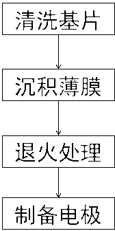
[0036] Step 1: Use K9 slide as substrate. Wipe the substrate with detergent and rinse with deionized water. Put the substrate into a container filled with acetone (analytical grade), put the container into an ultrasonic cleaner, ultrasonically clean it for 15 minutes, and then rinse the substrate with deionized water. Based on the same method, continue to use ethanol (analytical grade) and deionized water to clean the substrate in sequence. Put the cleaned substrate into a container filled with deionized water.

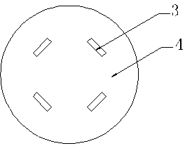
[0037] Step 2: Using a silicon-ruthenium composite target with a diameter of 100mm and a thickness of 3mm, six pure ruthenium blocks with a size of 4mm×15mm×1mm are symmetrically inlaid on the sputtering track of the silicon target; the area of ​​the ruthenium block and the sputtering track of the silicon target The ratio is about 6%.

[0038] Step 3: Use a mechanical pump to evacuate to below 3Pa, and then use a molecular pump to evacuate to 10 -4 Below Pa, and h...

Embodiment 2

[0045] Step 1: Same as Step 1 of Example 1.

[0046] Step 2: Using a silicon-ruthenium composite target with a diameter of 100mm and a thickness of 3mm, four pure ruthenium blocks with a size of 4mm×15mm×1mm are symmetrically embedded on the sputtering track of the silicon target. The ratio of the ruthenium bulk to the sputtering track area of ​​the silicon target is about 4%.

[0047] Step 3: Same as Step 3 of Example 1.

[0048] Step 4: Same as Step 4 of Example 1.

[0049] Step 5: Same as Step 5 of Example 1.

[0050] The measured thickness d of the obtained silicon-ruthenium alloy film was 864 nm, the length L was 4 mm, and the width W was 7 mm. The test results at room temperature are shown in Table 2, in which the conductivity and TCR of the intrinsic amorphous silicon film are obtained from reference materials, and the film square resistance is calculated at the same thickness d.

[0051] Table 2

[0052] Amorphous silicon based thin film Film conductiv...

Embodiment 3

[0054] Step 1: Same as Step 1 of Example 1.

[0055] Step 2: Using a silicon-ruthenium composite target with a diameter of 100mm and a thickness of 3mm, two pure ruthenium blocks with a size of 4mm×15mm×1mm are symmetrically embedded on the sputtering track of the silicon target. The ratio of the ruthenium bulk to the sputtering track area of ​​the silicon target is about 2%.

[0056] Step 3: Same as Step 3 of Example 1.

[0057] Step 4: Same as Step 4 of Example 1.

[0058] Step 5: Same as Step 5 of Example 1.

[0059] The measured thickness d of the obtained silicon-ruthenium alloy film was 770 nm, the length L was 4 mm, and the width W was 7 mm. The test results at room temperature are shown in Table 3, in which the conductivity and TCR of the intrinsic amorphous silicon film are obtained from reference materials, and the square resistance is obtained by calculation at the same thickness d.

[0060] table 3

[0061] Amorphous silicon based thin film Film co...


PUM

PropertyMeasurementUnit
Thicknessaaaaaaaaaa
Lengthaaaaaaaaaa
Widthaaaaaaaaaa

Abstract

The invention discloses a method for improving the electric conductivity of an amorphous silicon membrane, and belongs to the technical field of amorphous silicon membrane materials and apparatuses. The method comprises the following steps: (1) cleaning an insulating substrate; (2) depositing an amorphous ruthenium alloy film on the surface of the substrate by silicon-ruthenium composite target sputtering; (3) carrying out in-situ annealing treatment; and (4) preparing a metal electrode by adopting a copular electrode method. According to the method for improving electric conductivity of the amorphous silicon membrane disclosed by the invention, noble metal ruthenium is introduced to an amorphous network, so that the electric conductivity of the amorphous silicon membrane is effectively improved when the higher resistor temperature coefficient and good optical adsorption characteristics of the amorphous silicon membrane are kept. The method can be used for the fields such as thermistors, infrared detectors, silicon-based film solar cells, and the like.

Description

technical field [0001] The invention belongs to the technical field of silicon-based amorphous semiconductor thin film materials and devices, and in particular relates to a method for improving the electrical conductivity of an amorphous silicon thin film. Background technique [0002] Unlike traditional crystalline materials, amorphous semiconductor materials do not have long-range order, but a covalent random network structure without the constraints of periodic arrangement. Therefore, amorphous semiconductor materials have different characteristics from crystalline semiconductors in terms of optics and electricity. Amorphous silicon (a-Si) thin films have high light absorption rate, relatively large temperature coefficient of resistance (TCR), controllable band gap, large-area low-temperature (<400°C) film formation, unlimited types of substrates, and production It has outstanding advantages such as simple process and compatibility with silicon semiconductor process, ...

Claims


Application Information

Patent Timeline
IPC IPC(8): C23C14/06C23C14/35
Inventor 李伟郭安然何剑王垠余峰王冲蒋亚东
Owner UNIV OF ELECTRONIC SCI & TECH OF CHINA
Why Eureka
Try Eureka