
Surface acoustic wave device of multilayer film structure and preparation method thereof

A surface acoustic wave device and multi-layer film technology, applied in the direction of electrical components, impedance networks, etc., can solve the problems of restricting the frequency of SAW devices, high price, low phase velocity of surface acoustic waves, etc., and is conducive to large-scale promotion and application , The process conditions are convenient and easy to implement, and the effect of high electromechanical coupling coefficient

Inactive Publication Date: 2013-06-05
TIANJIN UNIVERSITY OF TECHNOLOGY
View PDF3 Cites 8 Cited by
  • Summary
  • Abstract
  • Description
  • Claims
  • Application Information

AI Technical Summary

Problems solved by technology

[0003] However, for conventional SAW materials such as quartz, zinc oxide, and lithium niobate, the surface velocity of the surface acoustic wave is low, and both are lower than 4000m / s. The finger width d of the finger transducer (IDT) must be less than 0.4um. If the center frequency is increased to 5GHz, the IDT finger width d corresponding to the surface acoustic wave device must be less than 0.2um, which is no different from the current semiconductor industry level. It is a great challenge, and with the reduction of the IDT finger width d, various problems such as severe finger breakage, poor reliability, low yield, and high price will be encountered in production, which seriously restricts the further development of the frequency of SAW devices. improve
At the same time, the reduction of IDT finger width will increase its resistance and generate a lot of heat. If the heat cannot be dissipated, the power that the device can withstand will be reduced. Therefore, devices made of conventional surface acoustic wave device materials cannot meet the requirements. Modern SAW devices with high frequency, high power and high electromechanical coupling coefficient

Method used


Image

  • Surface acoustic wave device of multilayer film structure and preparation method thereof
  • Surface acoustic wave device of multilayer film structure and preparation method thereof

Examples


Embodiment

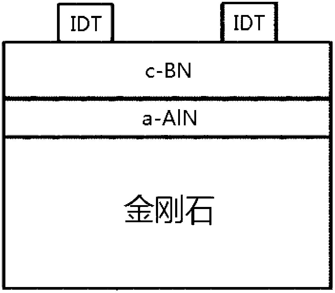
[0022] A surface acoustic wave device with a multilayer film structure, such as figure 1 As shown, the diamond is composed of CVD diamond film, a-axis preferentially oriented aluminum nitride (a-AlN) film, c-axis preferentially oriented boron nitride (c-BN) film and interdigital transducer (IDT). -Composite film structure, the thickness of described CVD diamond film is 20um, the thickness of a-AlN film is 300nm, the thickness of c-BN film is 400nm; Its preparation method comprises the following steps:

[0023] 1) Plasma treatment is performed on the surface of CVD diamond film to form a plasma-cleaned CVD diamond film surface. The specific method is: in the MOCVD deposition system, the surface of CVD diamond film is subjected to plasma treatment in a mixed gas atmosphere of nitrogen and argon , the nitrogen-argon volume flow ratio is 2:10, the filament voltage is 80V, the accelerating voltage is 100V, the temperature is 500°C, and the treatment time is 20min; this treatment ca...


PUM


Abstract

A surface acoustic wave device of a multilayer film structure comprises a CVD diamond film, an a-AlN film of axle a preferred orientation, a c-BN film of axle c preferred orientation and an interdigital transducer (IDT) in a successive superposition mode to form a diamond-complex film structure, wherein the thickness of the CVD diamond film is 20-25 micrometers, the thickness of the a-AlN film is 300-500nm, the thickness of the c-BN film is 300-500nm, the thickness of the IDT is 100nm, and the IDT is an aluminium film. The surface acoustic wave device of the multilayer film structure has the advantages that hardness and sound velocity of the diamond are high, high sound velocity of the a-AlN can effectively relieve a sound velocity frequency dispersion effect caused by big difference of the sound velocity between the diamond and the c-BN and a high electromechanical coupling coefficient of the c-BN. The surface acoustic wave device of the multilayer film structure can be used for manufacturing surface acoustic wave (SAW) devices which are high in frequency, high in sound velocity, high in power and high in electromechanical coupling coefficients.

Description

technical field [0001] The invention relates to the technical field of surface acoustic wave devices, in particular to a surface acoustic wave device with a multilayer film structure and a preparation method thereof. Background technique [0002] In recent years, high-frequency SAW filters have been widely used in intermediate frequency (IF) filtering of 3G digital mobile communication high-frequency systems. However, with the increasing shortage of radio communication frequency band resources, the frequency band below 2.5 GHz has been fully occupied, and only high-power and miniaturized surface acoustic wave (SAW) devices operating in the high-frequency band (2.5-10 GHz) can meet the needs of mobile communication systems. and bandwidth requirements of optical communication systems. Therefore, the development of high frequency (above 2.5GHz) SAW filters is imminent. [0003] However, for conventional SAW materials such as quartz, zinc oxide, and lithium niobate, the phase ...

Claims


Application Information

Patent Timeline
Patent Type & Authority Applications(China)
IPC IPC(8): H03H3/08H03H9/25H03H9/02
Inventor 陈希明李福龙薛玉明朱宇清张倩阴聚乾郭燕孙连婕
Owner TIANJIN UNIVERSITY OF TECHNOLOGY
Learn More