Inductive coupling plasma coil and plasma injection device

A plasma and inductive coupling technology, applied in the direction of circuits, discharge tubes, electrical components, etc., can solve the problems of polluting wafers, increasing quartz window sputtering, plasma radial and azimuth inhomogeneity, etc., and achieve low radio frequency voltage , reduce the coil, reduce the effect of standing wave effect

Active Publication Date: 2013-06-19
INST OF MICROELECTRONICS CHINESE ACAD OF SCI
View PDF3 Cites 2 Cited by
  • Summary
  • Abstract
  • Description
  • Claims
  • Application Information

AI Technical Summary

Problems solved by technology

[0006] The purpose of the present invention is to overcome the existing inductively coupled plasma implantation equipment with the increase of the size of the sample, the size of the plasma coil increases accordingly, and the excessive inductance increases the voltage at both ends of the coil, thereby causing the sputtering of the quartz window to contaminate the wafer , and due to the existence of the standing wave effect, the plasma produces radial and azimuthal inhomogeneity, which has many adverse effects on the semiconductor process.

Method used


Image

  • Inductive coupling plasma coil and plasma injection device
  • Inductive coupling plasma coil and plasma injection device
  • Inductive coupling plasma coil and plasma injection device

Examples


Embodiment Construction

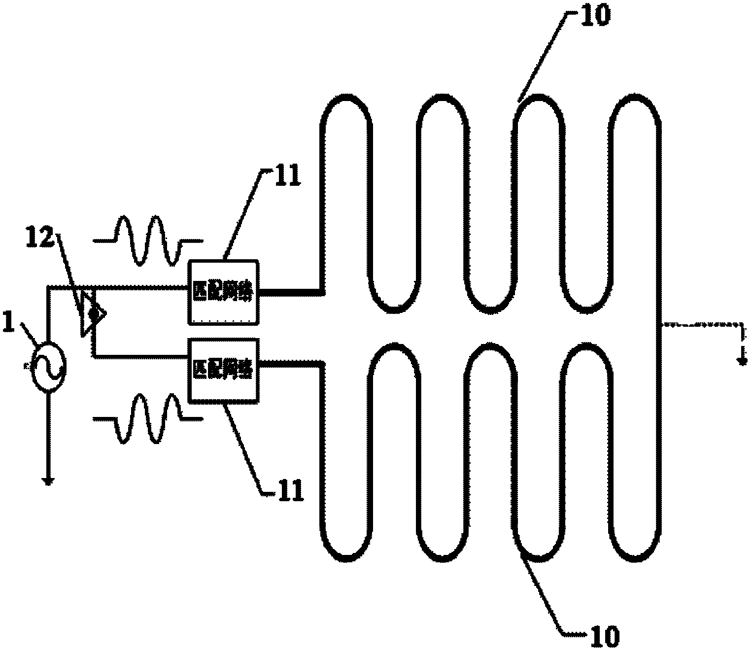
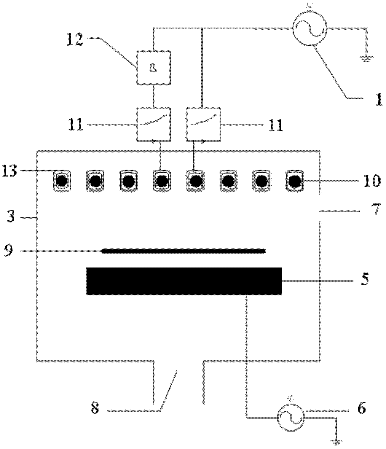
[0031] Such as figure 2 , image 3 As shown, the present invention provides an inductively coupled plasma coil 10 composed of two sets of folded radio frequency coils, one end of which is connected and the other end is not connected. The spatial structure of the two sets of radio frequency coils adopts a planar serpentine parallel connection, and the spatial distribution is strictly symmetrical, so that the direction of the radio frequency current at the same coil position is the same. The two sets of coils are made of hollow copper tubes with a radius of 1mm-10mm, which can be selected according to different requirements. In this embodiment, 5mm hollow copper tubes are used.

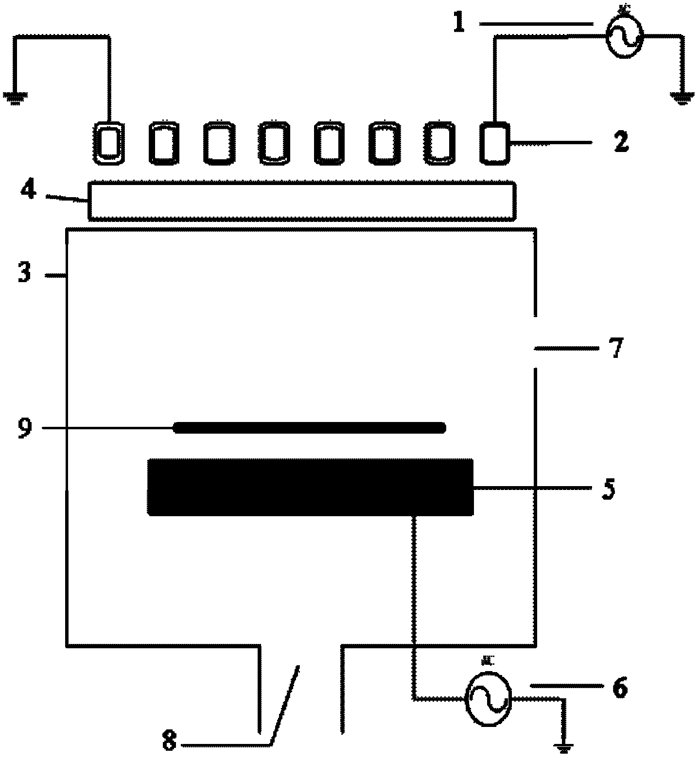
[0032] combine figure 2 , image 3 As shown, an inductively coupled plasma injection device provided by the present invention includes: plasma coil 10, two matching networks 11, phase shifter 12, quartz tube 13, first complementary power source 1, reaction chamber 3, base Seat 5 and second RF bias...


PUM


Abstract

The invention discloses an inductive coupling plasma coil which comprises two groups of radio-frequency coils formed in a back-bending mode. A plane S-shaped parallel connection way is adopted in space structures of two groups of the radio-frequency coils, and two groups of the radio-frequency coils are strictly symmetrical in space distribution so that the directions of radio frequency current of the same coil position are the same. The invention further discloses an inductive coupling plasma injection device provided with the inductive coupling plasma coil. According to the inductive coupling plasma coil and the injection device, on one hand, standing wave effect in the coil can be reduced and uniformity of plasma can be increased, and on the other hand, impedance matching can be well achieved, coupling effect of the plasma is increased, the probability of chip pollution caused by sputtering of a quartz window due to over-high voltage is lowered, the uniform high-density plasma of a large area can be generated in a reaction cavity of a large area, and therefore requirements of laboratory rooms and industry in the micro electronics field are met.

Description

technical field [0001] The invention belongs to the technical field of semiconductor processing equipment, in particular to an inductively coupled plasma coil and a plasma injection device. Background technique [0002] Plasma devices are widely used in ion implantation, etching and thin film deposition processes. With the continuous development of integrated circuit technology, especially flat panel display equipment, the plasma source is required to have good characteristics such as high density and large area uniformity. [0003] ICP inductively coupled plasma source has the advantages of high density, independent control of ion energy and density, and simple equipment, and has been widely used in integrated circuit technology. ICP Inductively Coupled Plasma typically uses coils for plasma excitation at low pressure. The ICP device supplies high-frequency power to the coil to generate an alternating electromagnetic field, and the electromagnetic field couples through th...

Claims


Application Information

Patent Timeline
Patent Type & Authority Applications(China)
IPC IPC(8): H01J37/32
Inventor 窦伟李楠李超波夏洋
Owner INST OF MICROELECTRONICS CHINESE ACAD OF SCI
Why Eureka
Try Eureka