Parallel connection double-junction solar cell

A technology of solar cells and parallel connection, which is applied in the field of solar cells, can solve problems such as complex preparation processes, and achieve the effect of ensuring heavy doping

Inactive Publication Date: 2013-06-19
NANTONG UNIVERSITY
View PDF2 Cites 4 Cited by
  • Summary
  • Abstract
  • Description
  • Claims
  • Application Information

AI Technical Summary

Problems solved by technology

This kind of parallel stacked battery needs to change the doping concentration layer by layer, which makes the preparation process of the battery v

Method used


Image

  • Parallel connection double-junction solar cell
  • Parallel connection double-junction solar cell
  • Parallel connection double-junction solar cell

Examples


Embodiment 1

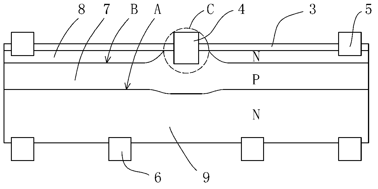
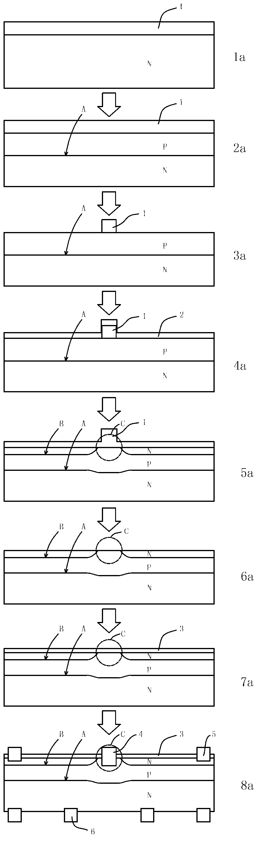
[0040] Such as image 3 As shown, it is a schematic diagram of the manufacturing process flow of the parallel double-junction solar cell of the present invention, and the specific steps of the process are as follows:

[0041] 1a, use magnetron sputtering to deposit a silicon dioxide film 1 with a thickness of about 0.05 microns on the upper surface of the silicon wafer 9 after texturing, and the concentration of boron in the silicon dioxide film 1e19 / cm3 ;

[0042] 2a. Diffusion the deposited silicon wafer at high temperature, so that the doping element (boron) in the silicon dioxide film 1 diffuses into the silicon wafer to form a PN deep junction A;

[0043] 3a. Removing the oxide layer (silicon dioxide film 1) other than the top electrode area on the upper surface of the silicon wafer 9;

[0044] 4a. Depositing an intrinsic amorphous silicon layer 2 on the upper surface of the silicon wafer, the thickness of the deposited intrinsic amorphous silicon layer is about 40nm; ...

Embodiment 2

[0050] The steps of this embodiment are the same as those of Process Example 1, the difference lies in the process parameters of high-temperature diffusion in dry oxygen environment in step 5a (the fifth step). In this embodiment, the process temperature of high-temperature diffusion is 1000°C, and the duration is 5 minute.

Embodiment 3

[0052] The steps of this embodiment are the same as those of Process Example 1, the difference lies in the process parameters of high-temperature diffusion in dry oxygen environment in step 5a (step 5). In this embodiment, the process temperature of high-temperature diffusion is 1100°C, and the duration is 2 minute.

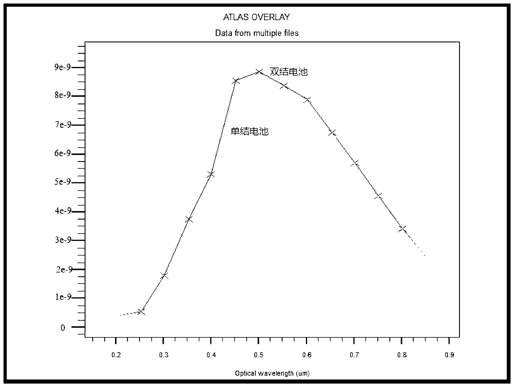
[0053] After simulating the above three process embodiments, it is found through comparison that the PN junction of the battery is continuously deepened with the increase of the high temperature diffusion temperature of the reverse diffusion process. The impurity concentration on the surface of the battery first increases and then decreases, but the impurity concentration in the top electrode region gradually increases with the increase of temperature. The heavily doped impurities in the top electrode region mainly diffuse into the battery body, and the lateral diffusion is small. This is related to the deposition of the intrinsic amorphous silicon layer on the s...


PUM

PropertyMeasurementUnit
Thicknessaaaaaaaaaa
Thicknessaaaaaaaaaa

Abstract

The invention relates to a parallel connection double-junction solar cell. The parallel connection double-junction solar cell comprises a silicon slice, a deep junction and a shallow junction are sequentially arranged on one side of the upper surface of the silicon slice from inside to outside to form a P-N-P type or N-P-N type double-junction cell, doping elements of the cell are diffused in a first crystal silicon layer between the deep junction and the shallow junction, the first crystal silicon layer extends to a top electrode area from inside to outside, the top electrode area is a heavy doping area, a second crystal silicon layer with electrical properties opposite to those of the doping elements is arranged above the shallow junction, the second crystal silicon layer is located outside the top electrode area on the upper surface of the silicon slice, a top electrode is in ohmic contact with the first crystal silicon layer, a transoid electrode which is in ohmic contact with the second crystal silicon layer is arranged on a non-top-electrode area, and the transoid electrode is connected with a back electrode. According to the parallel connection double-junction solar cell, two PN junctions are formed in the same monocrystalline silicon battery and share one p area, the difficulty of current carriers in a series connection laminated cell to penetrate through a tunnel junction is reduced, the absorption of short waves is facilitated by the aid of the shallow junction, the absorption of long waves is effectively guaranteed by the aid of the deep junction, and thereby performances of the cell are good.

Description

technical field [0001] The invention relates to a parallel double-junction solar cell, which belongs to the technical field of solar cells. Background technique [0002] At present, solar cells mainly include monocrystalline silicon cells, polycrystalline silicon cells and thin-film cells, among which monocrystalline silicon cells have the highest mass production conversion efficiency, which can reach 18-19%. However, the conversion efficiency of the solar cell cannot meet people's demand for the conversion efficiency of the solar cell. Therefore, people have carried out corresponding structural design on the battery to further improve the conversion efficiency of the battery. In view of the fact that the absorption of solar energy by a single material is concentrated in a small wavelength, people have proposed the concept of stacked batteries, that is, batteries composed of multiple materials are stacked in series, so that the batteries corresponding to different materials...

Claims


Application Information

Patent Timeline
IPC IPC(8): H01L31/0687H01L31/18
CPCY02E10/544Y02P70/50
Inventor 王强花国然朱海峰宋长青
Owner NANTONG UNIVERSITY
Why Eureka
Try Eureka