Preparation method of large-area graphene on Si substrate based on Ni film annealing

A graphene and large-area technology, applied in the field of microelectronics, can solve problems such as low processing temperature, inappropriate production, and graphene film defects, and achieve the effects of low porosity, smooth surface, and good continuity

Inactive Publication Date: 2013-07-03
XIDIAN UNIV
View PDF3 Cites 6 Cited by
  • Summary
  • Abstract
  • Description
  • Claims
  • Application Information

AI Technical Summary

Problems solved by technology

Chemical vapor deposition method provides an effective method for the controllable preparation of graphene, and its biggest advantage is that it can prepare graphene sheets with large area. The disadvantage is that it must be completed at high t

Method used


Image

  • Preparation method of large-area graphene on Si substrate based on Ni film annealing
  • Preparation method of large-area graphene on Si substrate based on Ni film annealing

Examples


Embodiment 1

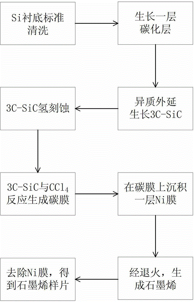
[0040] Example 1, preparing a graphene material based on Ni film annealing on a 4-inch Si substrate.

[0041] Step 1: Clean the 4-inch Si substrate with a mixed solution of ammonia water and hydrogen peroxide, and a mixed solution of hydrochloric acid and hydrogen peroxide in sequence.

[0042] (1.1) According to NH 4 OH:H 2 o 2 :H 2Prepare a solution at a ratio of O=1:2:5, place a 4-inch Si substrate in the solution, soak for 10 minutes, rinse with deionized water repeatedly, and then dry to remove organic residues on the surface of the sample;

[0043] (1.2) According to HCl: H 2 o 2 :H 2 A solution was prepared at a ratio of O=1:2:8, and a 4-inch Si substrate after removing surface organic residues was placed in the solution, soaked for 10 minutes, rinsed repeatedly with deionized water, and then dried to remove ionic pollutants .

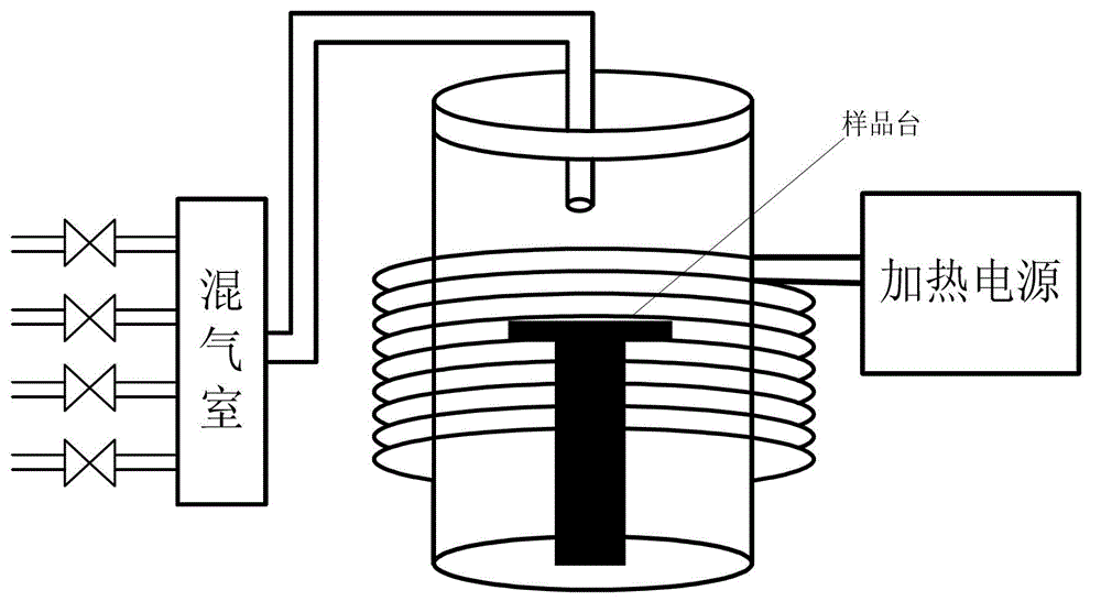
[0044] Step Two: Vacuum.

[0045] Put the Si substrate into the reaction chamber of the CVD system, and evacuate the reaction chamber ...

Embodiment 2

[0061] Example 2, preparing a graphene material based on Ni film annealing on an 8-inch Si substrate.

[0062] Step 1: Clean the 8-inch Si substrate with a mixed solution of ammonia water and hydrogen peroxide, and a mixed solution of hydrochloric acid and hydrogen peroxide in sequence.

[0063] The cleaning steps are the same as the first step in Example 1.

[0064] Step 2: Vacuum.

[0065] Put the Si substrate substrate into the reaction chamber of the CVD system, and evacuate the reaction chamber to 10 -7 mbar level.

[0066] Step 3: Grow the carbonized layer.

[0067] in H 2 In the case of protection, the temperature of the reaction chamber is raised to the carbonization temperature of 1100 ° C, and then the flow rate of 30ml / min is introduced into the reaction chamber. 3 h 8 , grow a layer of carbonized layer on the Si substrate, the growth time is 6min.

[0068] Step 4: growing a 3C-SiC epitaxial film on the carbonized layer.

[0069] Rapidly raise the temperatur...

Embodiment 3

[0081] Example 3, preparing a graphene material based on Ni film annealing on a 12-inch Si substrate.

[0082] Step 1: Clean the 12-inch Si substrate with a mixed solution of ammonia water and hydrogen peroxide, and a mixed solution of hydrochloric acid and hydrogen peroxide in sequence.

[0083] The cleaning steps are the same as the first step in Example 1.

[0084] Step 2: Put the Si substrate substrate into the reaction chamber of the CVD system, and evacuate the reaction chamber to 10 -7 mbar level.

[0085] Step 3: In H 2 In the case of protection, the temperature of the reaction chamber is raised to the carbonization temperature of 1200 ° C, and then the flow rate of 30ml / min is introduced into the reaction chamber. 3 h 8 , for 4 min to grow a carbonized layer on the Si substrate.

[0086] Step 4: Rapidly raise the temperature of the reaction chamber to the growth temperature of 1350°C, and feed SiH at a flow rate of 35ml / min respectively 4 and C with a flow rate ...


PUM


Abstract

The invention discloses a preparation method of large-area graphene on an Si substrate based on Ni film annealing and mainly solves the problems of small area, poor continuity and non-uniform layers of graphene prepared in the prior art. The preparation method comprises the following implementation steps: growing a carburization layer on the 4-12-inch Si substrate to be used as a transition and growing a 3C-SiC heteroepitaxial film at the temperature of 1200 DEG C to 1350 DEG C by utilizing growth gas sources C3H8 and SiH4; carrying out hydrogen etching on the grown 3C-SiC film and removing a compound generated by etching; reacting 3C-SiC with gaseous CCl4 at a temperature of 800-1,000 DEG C to generate a carbon film; electron beam-depositing an Ni film on the carbon film, putting a sample sheet plated with the Ni film into Ar gas and annealing for 10-20 minutes at a temperature of 1,000-1,250 DEG C to generate a graphene sample sheet; and finally removing the Ni film from the graphene sample sheet. The graphene prepared by the method has the advantage that the area can reach 12 inches, the continuity is good, the surface is smooth, and the porosity is low. The graphene can be used for manufacturing microelectronic devices and biological sensors or sealing gas and liquid.

Description

technical field [0001] The invention belongs to the technical field of microelectronics, and relates to a semiconductor material and a preparation method thereof, in particular to a method for preparing large-area graphene on a Si substrate based on Ni film annealing. technical background [0002] Graphene is a new carbonaceous material formed by dense packing of carbon atoms into a honeycomb lattice structure. 2 Hybrid carbon, that is, the basic structural unit of carbon connected by double bonds or other atoms, has some special physical properties, including: unique carrier characteristics; electrons transport in graphene with little resistance and move at sub-micron distances There is no scattering at the time, and it has good electron transport properties; good mechanical properties and good toughness, and the maximum pressure per 100nm distance can reach 2.9N; the unique energy band structure of graphene separates holes and electrons from each other, resulting in new el...

Claims


Application Information

Patent Timeline
IPC IPC(8): C01B31/04C01B32/184
Inventor 郭辉胡彦飞张玉明张丰雷天民
Owner XIDIAN UNIV
Why Eureka
Try Eureka