Solar battery doped region forming method

A technology of solar cells and doped regions, applied in the field of photovoltaic doping, can solve the problems of high activation cost, complicated process, high quality requirements of silicon wafers, etc., and achieve the effects of simplified process conditions, low temperature and fast response speed

Inactive Publication Date: 2013-07-03
WUXI SUNTECH POWER CO LTD
View PDF2 Cites 5 Cited by
  • Summary
  • Abstract
  • Description
  • Claims
  • Application Information

AI Technical Summary

Problems solved by technology

[0006] The invention provides a method for forming a doped region of a solar cell, with the purpose of solving the problems of high-temperature activation on silicon wafer quality, complicated process and high activation cost

Method used


Image

  • Solar battery doped region forming method
  • Solar battery doped region forming method
  • Solar battery doped region forming method

Examples


Embodiment 1

[0038] Embodiment 1: The method for forming the doped region of the solar cell

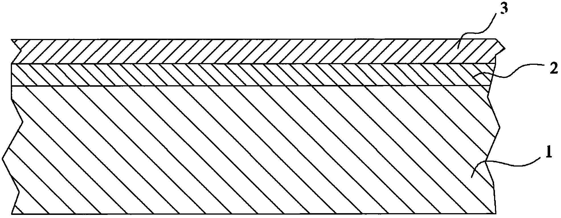
[0039] See attached figure 1 , attached figure 2 And attached image 3 As shown, a method for forming a doped region of a solar cell is used to prepare a selective emitter solar cell, and the specific operation steps are:

[0040] ①. Select a P-type single crystal silicon wafer 1 with a resistivity of 0.5-3Ω·cm. In a mixed solution of NaOH and isopropanol, at a temperature of 90°C, etch the surface of the silicon wafer to obtain a uniform size. After the suede surface, soak it in dilute hydrochloric acid and hydrofluoric acid solution for 5 minutes, and finally rinse it with deionized water and dry it.

[0041] ②, using a conventional diffusion furnace (conventional thermal diffusion process), using phosphorus oxychloride (POCl 3 ) Diffusion of phosphorus on the surface of the silicon wafer. During the diffusion, the silicon wafers are placed back to back on the quartz boat. The constant temp...

Embodiment 2

[0053] Embodiment 2, the method for forming the doped region of the solar cell

[0054] See attached Figure 4 , attached Figure 5 And attached Image 6 As shown, a method for forming a doped region of a solar cell, the back contact structure of the solar cell prepared by this method, the specific operation steps are:

[0055] ①. According to the steps ①, ②, and ③ in Example 1, silicon wafers were prepared.

[0056] ②, as attached Figure 4 As shown, a layer of silicon dioxide is formed on the back surface of the P-type single crystal silicon wafer 1 as the passivation layer 3 . This step is to form a passivation layer on the surface (whole surface) of a semiconductor substrate (silicon wafer).

[0057] ③. Perform ion implantation of boron (B) dopant on the back surface of the silicon wafer, and the dopant may also be aluminum (Al), gallium (Ga), or indium (In) of the same family as boron. This step is to use ion implantation to pass through the passivation layer (silic...
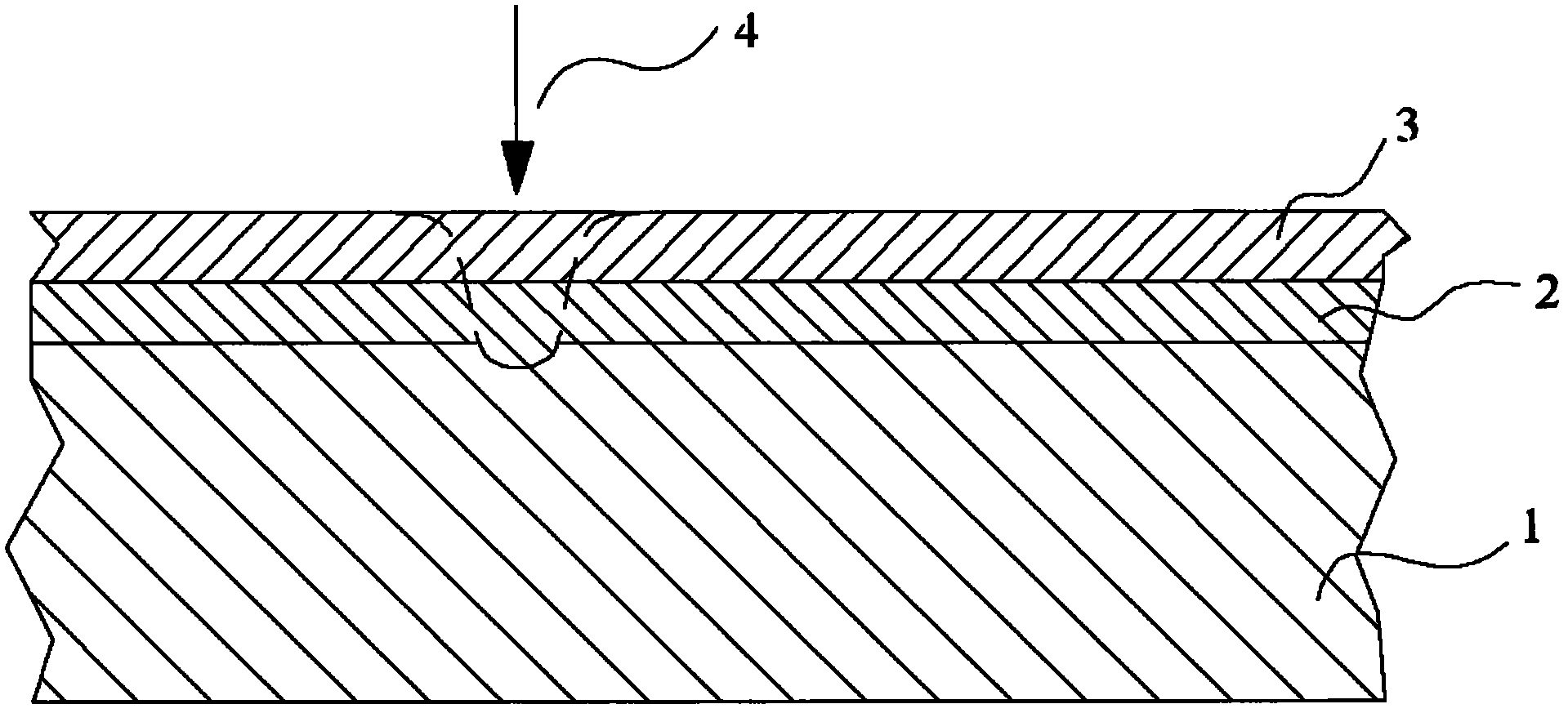
Embodiment 3

[0063] Embodiment 3, the method for forming the doped region of the solar cell

[0064] Laser activation is used to simultaneously prepare the selective emitter (the method is the same as in Example 1) and the back partial contact (the method is the same as in Example 2).

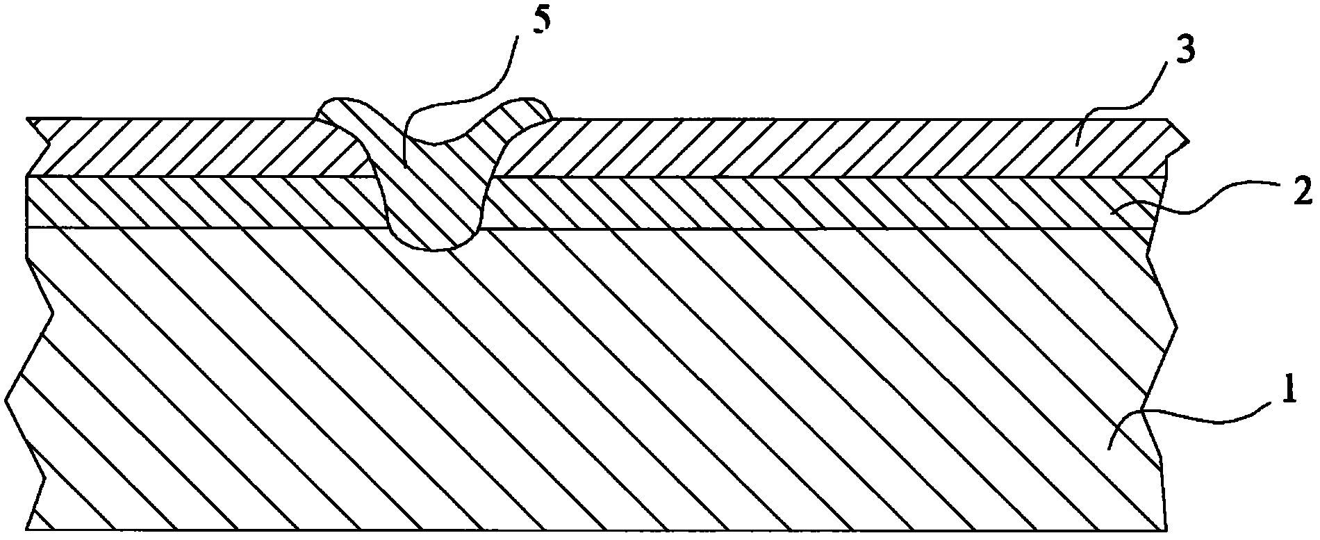
[0065] On the basis of the above two embodiments, a solar cell with both a front selective emitter and a rear partial contact structure can be formed on a silicon wafer. The schematic diagram of its structure is shown in the attached Figure 7 shown.

[0066] The power of the laser used is 3W; the speed of the laser is 5000mm / s.


PUM

PropertyMeasurementUnit
thicknessaaaaaaaaaa
thicknessaaaaaaaaaa
wavelengthaaaaaaaaaa

Abstract

A solar battery doped region forming method comprises the following steps: (1) forming a passivation layer on the surface of a semiconductor substrate; (2) adopting an ion implantation method, penetrating the passivation layer and forming an impurity source region on the semiconductor substrate; and (3) irradiating the impurity source region by using laser to enable the impurity source region to activate and obtaining the solar battery doped region. According to the solar battery doped region forming method, the laser is used for activating the doped region, due to the facts that regulation of the speed and power of the laser is convenient and fast, and response speed is fast, accurate control to dosage concentration, dosage depth and doped region width is achieved, and technological conditions are simplified.

Description

technical field [0001] The invention relates to a method for forming a doped region of a solar cell, in particular to a method for forming a doped region or a selectively doped region of a solar cell by laser activating an ion-implanted impurity source, the method comprising forming an N-type doped region on a solar cell Doping (n++) regions or forming P-type doping (p++) regions belongs to the field of photovoltaic doping technology. Background technique [0002] Due to the limited supply of conventional energy and the increase in environmental protection pressure, many countries in the world have set off an upsurge in the development and utilization of solar energy and renewable energy, and solar energy utilization technology has developed rapidly. The application of electric energy is more and more extensive. The solar cell is one of the most common devices used to convert solar energy into electrical energy. In practical applications, the basic application unit is gene...

Claims


Application Information

Patent Timeline
Patent Type & Authority Applications(China)
IPC IPC(8): H01L31/18B23K26/00B23K26/53
CPCY02P70/50
Inventor 王振交韩培育金光耀陆红艳
Owner WUXI SUNTECH POWER CO LTD
Why Eureka
Try Eureka