Semi-insolating GaAs photoconductive antenna with ohmic contact electrodes

An ohmic contact electrode, photoconductive antenna technology, applied in the direction of antenna, antenna support/installation device, electrical components, etc., can solve the problem of low emission efficiency of photoconductive antenna, improve radiation efficiency and radiation power, and improve emission efficiency , the effect of increasing the breakdown electric field

Inactive Publication Date: 2013-08-07
XIAN UNIV OF TECH +1
View PDF4 Cites 4 Cited by
  • Summary
  • Abstract
  • Description
  • Claims
  • Application Information

AI Technical Summary

Problems solved by technology

[0004] The purpose of the present invention is to provide a semi-insulated GaAs photoconductive antenna with ohmic contact electrodes, which solves the problem of low emission efficiency of existing photoconductive antennas

Method used


Image

  • Semi-insolating GaAs photoconductive antenna with ohmic contact electrodes
  • Semi-insolating GaAs photoconductive antenna with ohmic contact electrodes
  • Semi-insolating GaAs photoconductive antenna with ohmic contact electrodes

Examples


Embodiment Construction

[0024] The present invention will be further described in detail below in conjunction with the accompanying drawings and specific embodiments.

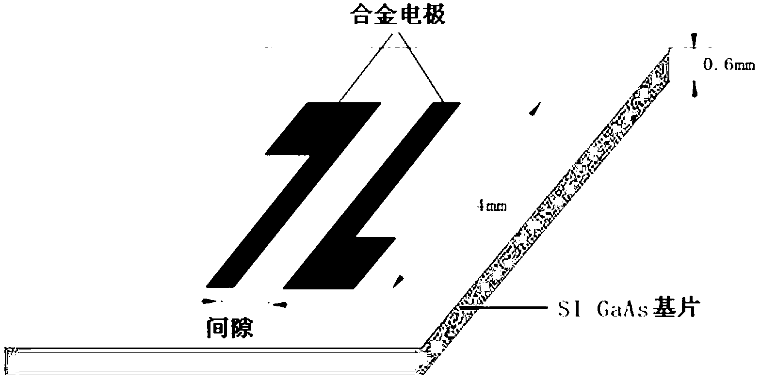
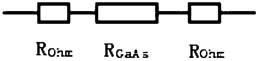
[0025] see figure 1 , the present invention has the semi-insulated GaAs photoconductive antenna of AuGeNi alloy ohmic contact electrode, comprises semi-insulated gallium arsenide substrate, on the semi-insulated gallium arsenide substrate are positive and negative two AuGeNi alloy electrodes, semi-insulated gallium arsenide substrate It can be regarded as a resistor R with a large resistance GaAs , the contact resistance between the two AuGeNi alloy electrodes and the substrate material can be regarded as two resistors with small resistance R Ohm , resistor R GaAs with two resistors R Ohm in series, R Ohm GaAs . Resistance R GaAs The resistance value is from several megohms to hundreds of megohms, while R Ohm The resistance is less than 1 ohm. due to R Ohm GaA , s R Ohm Ignorable.

[0026] The substrate material of the pho...


PUM

PropertyMeasurementUnit
electrical resistivityaaaaaaaaaa

Abstract

A semi-insulating GaAs photoconductive antenna with ohmic contact electrodes comprises a semi-insulating GaAs substrate which is provided with a positive AuGeNi alloy electrode and a negative AuGeNi alloy electrode; the semi-insulating GaAs substrate can be considered as a resistor RGaAs with high resistance; the two AuGeNi alloy electrodes can be considered as the resistors Rohm with lower resistance; the resistor RGaAs is connected with the resistors Rohm in serials; and Rohm << RGaAs. Breakdown electric field of the photoconductive antenna is increased through ohmic contact of the antenna electrodes, and meanwhile the whole gap between the electrodes is basically or totally covered by the electric field distribution of the antenna; and as intensity of photon-generated carriers of a unit area is decreased, coulomb screening effect and radiation-field screening effect are controlled effectively, and emitting efficiency of the antenna is increased. Compared with those of the traditional antennas, radiation efficiency and radiation power of the photoconductive antenna with the AuGeNi alloy ohmic contact electrodes are remarkably increased.

Description

technical field [0001] The invention belongs to the interdisciplinary field of ultra-high-speed electronics, ultra-fast optics, and terahertz science and technology, and relates to a semi-insulated GaAs photoconductive antenna with ohmic contact electrodes. Background technique [0002] Terahertz waves generally refer to electromagnetic radiation with a frequency in the range of 0.1 THz to 10 THz (wavelength in the range of 3 mm to 30 um). Compared with other bands, terahertz electromagnetic waves have their unique properties, such as transient, broadband, coherence and low energy, etc. Fields such as military radar have important scientific value and broad application prospects. [0003] The radiation mechanism of the photoconductive antenna is that the photogenerated carriers excited by the laser pulse are accelerated under the action of the external bias electric field and the built-in electric field, thereby generating a transient photocurrent on the surface of the phot...

Claims


Application Information

Patent Timeline
Patent Type & Authority Applications(China)
IPC IPC(8): H01Q23/00H01Q1/22
Inventor 侯磊董陈岗杨汇鑫施卫陈素果闫志巾
Owner XIAN UNIV OF TECH
Why Eureka
Try Eureka