Graphene field effect transistor

A field-effect transistor and graphene technology, which is applied in the direction of transistors, semiconductor devices, electrical components, etc., can solve the problems of reduced mobility, difficult performance, and low device efficiency

Inactive Publication Date: 2013-08-14
李德杰
View PDF6 Cites 26 Cited by
  • Summary
  • Abstract
  • Description
  • Claims
  • Application Information

AI Technical Summary

Problems solved by technology

Even for analog devices, the high conductivity and nonlinearity lead to devices that are too inefficient and require some degree of passivation to reduce their conductivity
Passivation can lead to a significant decrease in mobility. Compared with conventional semiconductor devices, the advantage is not great, but the process is very difficult
[0004] The above-mentioned contradictions in graphene cannot be completely overcome in fact. It is difficult for semiconductor field effect devices using graphene as the active layer to exceed the performance of existing semiconductor devices. It is even more difficult to replace silicon for large-scale integrated circuits. And that's it

Method used


Image

  • Graphene field effect transistor
  • Graphene field effect transistor
  • Graphene field effect transistor

Examples


Embodiment 1

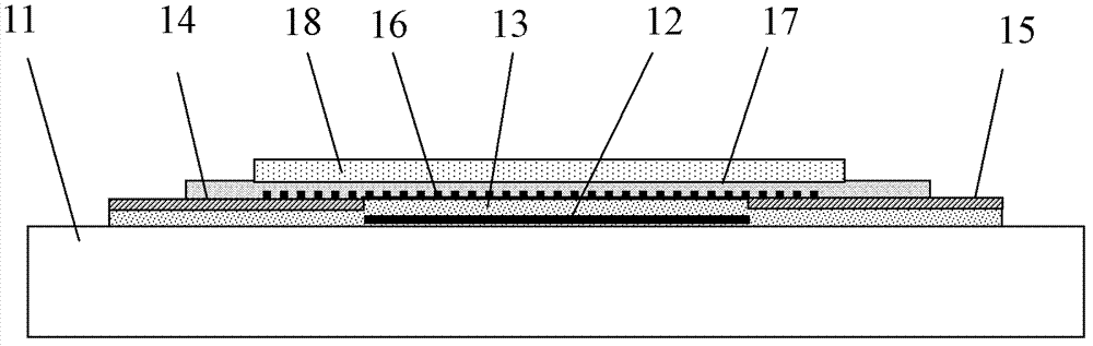
[0028] Bottom gate structure, the substrate is a semi-insulating silicon wafer, on which the metal chromium-palladium composite thin film gate is first prepared, and then the aluminum oxide / strontium barium fluoride insulating layer is prepared, wherein the thickness of aluminum oxide is 50 nanometers, and the thickness of strontium fluoride is 10 nanometers . Barium strontium fluoride is lattice-matched with graphene, and a single layer of graphene is deposited on it by CVD method, and the source and drain are prepared simultaneously. Graphene is passivated in an isochlorine plasma, and then a semiconductor layer of zirconium nitride and a protective layer of aluminum oxide are deposited on it to form a complete device.

Embodiment 2

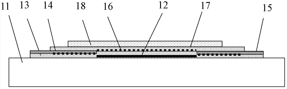
[0030] Bottom gate structure, the substrate is a semi-insulating silicon wafer, on which a metal chromium-gold composite thin film gate is first prepared, and then an aluminum oxide / hafnium oxide insulating layer is prepared, wherein the thickness of aluminum oxide is 20 nanometers, and the thickness of hafnium oxide is 10 nanometers. Single-layer graphene is deposited on hafnium oxide by CVD method, and the source and drain are prepared simultaneously. Graphene was passivated in a bromine plasma, and then a semiconductor layer of cadmium sulfide and a protective layer of aluminum oxide were deposited on it to form a complete device.

Embodiment 3

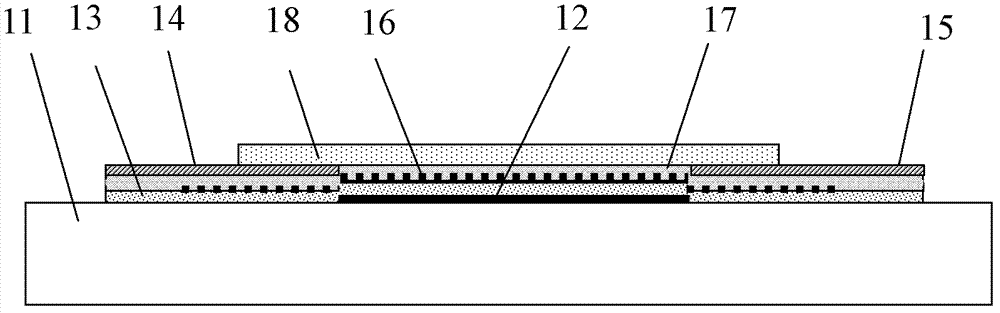
[0032] Top-gate structure, the substrate is an insulating silicon carbide wafer, on which an n-type silicon semiconductor layer is first prepared, and a single-layer graphene is prepared on a copper foil by CVD, and then transferred to the n-type silicon semiconductor layer and subjected to hydrogenation treatment. After the metal source and drain are prepared, a hafnium oxide / alumina insulating layer is prepared, wherein the thickness of aluminum oxide is 20 nanometers, and the thickness of hafnium oxide is 6 nanometers. Finally, the top gate is prepared to form a complete device.


PUM


Abstract

The invention discloses a graphene field effect transistor, and belongs to the technical field of electronics and graphene. A basic structure of the graphene field effect transistor comprises a grid, a source, a drain, an insulation layer and an active layer, wherein the active layer is formed by compositing single-layer or multi-layer graphene with the insulator or semiconductor characteristic after passivation and other semiconductor materials. The graphene field effect transistor successfully overcomes the fatal defects of the existing graphene field effect tube, has the higher performance compared with the conventional semiconductor field effect tube, and can promote an application of the graphene in the technical field of the electronics.

Description

technical field [0001] The invention relates to a novel electronic device, in particular to a graphene field effect transistor, and belongs to the technical field of electronic devices and graphene. Background technique [0002] Graphene has been used as an electrode material in the field of electronic devices, such as touch screens and transparent conductive electrodes for photovoltaic cells. In terms of active electronic devices where people place the greatest hope, especially in the field of field effect thin film transistors, although extensive and in-depth research has been carried out, there has been little substantial progress. So far, improvement measures have mainly dealt with the insulating layer and the graphene layer. In terms of the insulating layer, an insulating layer with a non-polarized surface is mainly used. The specific method is to use a boron nitride film with a hexagonal structure as the insulating layer, or use an organic material to perform non-pola...

Claims


Application Information

Patent Timeline
Patent Type & Authority Applications(China)
IPC IPC(8): H01L29/786H01L29/12H01L29/10
Inventor 李德杰
Owner 李德杰
Why Eureka
Try Eureka