A power ldmos device with junction field plate

A junction field plate and device technology, applied in semiconductor devices, electrical components, diodes, etc., can solve the problems of reducing on-resistance, affecting the breakdown characteristics of devices, occupying the area of ​​current flow, etc., to reduce on-resistance, Improved breakdown characteristics and reduced reverse current

Inactive Publication Date: 2015-08-19
UNIV OF ELECTRONICS SCI & TECH OF CHINA +1
View PDF2 Cites 0 Cited by
  • Summary
  • Abstract
  • Description
  • Claims
  • Application Information

AI Technical Summary

Problems solved by technology

Literature (Chen Xingbi, [p-n + A simple expression of the surface electric field distribution when there is a field plate】, Electronic Journal, Vol.14, 36 (1986)) pointed out that the metal field plate (such as figure 1 shown) can effectively reduce the peak electric field on the surface of the device and improve the distribution of the electric field on the surface of the device, thereby increasing the breakdown voltage of the device; but the disadvantage of the metal field plate is that the end of the metal field plate will introduce an additional electric field peak and affect the breakdown of the device. wear characteristics
However, the RESURF structure needs to occupy part of the current flow area, which is not conducive to further reducing the on-resistance

Method used


Image

  • A power ldmos device with junction field plate
  • A power ldmos device with junction field plate
  • A power ldmos device with junction field plate

Examples


Embodiment approach 1

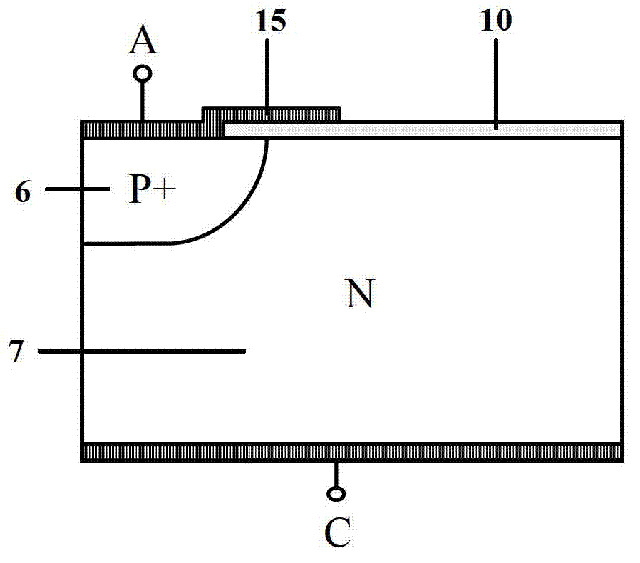
[0039] Figure 6 It is a schematic diagram of the structure of a power LDMOS device with JFP proposed by the present invention, including a substrate 1, an N buried layer 2, a P-type body region 4, a source region 5, a body contact region 6, an active layer 7, a drain region 8, and electrode isolation Dielectric layer 9, gate dielectric 10a, gate electrode conductive material 10b, P-type ohmic contact region 11, P-type high resistance region 12, N-type ohmic contact region 13, field dielectric 14, source electrode S, gate electrode G, and drain electrode D , where the active layer between the body region 4 and the drain region 8 is called the drift region.

[0040] The P-type ohmic contact region 11, the P-type high resistance region 12, the N-type ohmic contact region 13 and the field medium 14 form a junction field plate structure JFP located on the surface of the device; wherein the P-type ohmic contact region 11 is electrically connected to the source electrode S, The N-t...

Embodiment approach 2

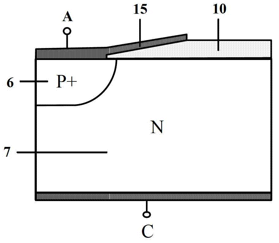
[0044] Figure 7 It is a schematic structural diagram of a JFP high-voltage LDMOS device with an N-type buffer zone 12c in a junction field plate proposed by the present invention; and Figure 6 Compared with the structure shown, an N-type buffer area 12c is added between the P-type high resistance region 12 and the N-type ohmic contact region 13, and the doping concentration of the N-type buffer region 12c is lower than that of the N-type ohmic contact region 13 . The added N-type buffer zone 12c can alleviate the electric field peak of the device between the N-type ohmic contact region 13 and the P-type semiconductor layer 12d, which is beneficial to improve the withstand voltage characteristics of the device.

Embodiment approach 3

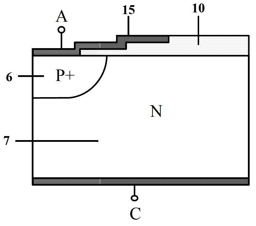
[0046] Figure 8 It is a schematic structural diagram of a JFP power LDMOS device provided by the present invention with a part of the buried layer 2 of the semiconductor of the second conductivity type. and Figure 6 Compared to the shown structure, Figure 8 The middle part of the N-type buried layer 2 is in the substrate 1 below the drain terminal. At this time, the N-type buried layer 2 can also improve the vertical withstand voltage of the device; at the same time, compared with the case of the entire N-type buried layer 2, the partial N-type buried layer 2 It is beneficial to reduce the substrate leakage current.


PUM


Abstract

The invention relates to a power LDMOS device with a junction field plate, and belongs to the technical field of power semiconductor devices. According to the power LDMOS device with the junction field plate, a buried layer opposite to a substrate doping type is formed on a substrate of a conventional LDMOS device, and the junction field plate formed by a PN junction is formed in the surface of a device drifting area. The power LDMOS device with the junction field plate uses PN junction electric field distribution in the junction field plate for modulating a device surface electric field, the distribution of the device surface electric field is made to be more even, the insufficiency of a peak of a tail end electric filed of a metal field plate can be effectively avoided, and breakdown performance of the device is improved. Under the reverse blocking state, the junction field plate has an auxiliary exhaustion function for the drifting area, the doping level of the drifting area can be improved to a large extent, and the on-resistance of the device is reduced. Meanwhile, reverse currents are small when reverse bias of the PN junction in the junction field plate occurs, the fact that leakage currents in the field plate are reduced is benefited, and the buried layer in the substrate can effectively improve the voltage endurance property of the device. The device has the advantages of being high in voltage, low in power consumption, low in cost and easy to integrate, and is suitable for power integrated circuits and radio frequency power integrated circuits.

Description

technical field [0001] The invention belongs to the technical field of power semiconductor devices, and relates to power MOSFET devices, especially power LDMOS devices. Background of the invention [0002] For conventional LDMOS devices, the length of the drift region increases monotonously with the increase of the breakdown voltage of the device; this not only increases the chip area and cost of the device (or circuit), but also is not conducive to chip miniaturization. More seriously, the on-resistance of the device increases with the increase of the length of the drift region (or the withstand voltage of the device), among which the breakdown voltage (BV, Breakdown Voltage) is related to the specific on-resistance (R on,sp , Specific on-Resistance) can be expressed as R on,sp ∝BV 2.5 , and the increase in on-resistance leads to a sharp increase in power consumption of the device, and the switching speed of the device is also reduced. [0003] In order to alleviate the ...

Claims


Application Information

Patent Timeline
Patent Type & Authority Patents(China)
IPC IPC(8): H01L29/78H01L29/40
CPCH01L29/7818H01L29/402H01L29/0634H01L29/1083
Inventor 罗小蓉魏杰罗尹春范远航徐青范叶王骁玮周坤张彦辉尹超张波李肇基
Owner UNIV OF ELECTRONICS SCI & TECH OF CHINA
Why Eureka
Try Eureka