Target material, preparation method thereof, and display device

A display device and target technology, which is applied in metal material coating process, ion implantation plating, coating and other directions, can solve the problem of incompetent high-resolution active display devices, etc. The effect of high carrier mobility

Active Publication Date: 2014-10-22
TRULY SEMICON
View PDF5 Cites 0 Cited by
  • Summary
  • Abstract
  • Description
  • Claims
  • Application Information

AI Technical Summary

Problems solved by technology

IGZO TFT is currently the most mature oxide TFT technology, although its carrier mobility is usually greater than 20cm 2 / Vs, which is higher than that of amorphous silicon TFT, but it is still not suitable for active display devices with high resolution and narrow frame integrated drive, especially the development requirements in the field of AMOLED

Method used


Image

  • Target material, preparation method thereof, and display device
  • Target material, preparation method thereof, and display device
  • Target material, preparation method thereof, and display device

Examples


Embodiment 1

[0071] Embodiments of the present invention provide a target material and a preparation method thereof. Specifically, the target material provided by the embodiment of the present invention has the atomic ratio shown in formula (I):

[0072] A a B b Ge c ZnO d (I),

[0073] Wherein, A and B are respectively any element in the elements Pb, Tl, Sn, Sb and Bi; the value ranges of a and b are both 0-100, including endpoint values, and a and b are not 0 at the same time, The value range of c is 0.01-100, including the endpoint value.

[0074] It should be noted that since the overall valence of the compound shown in formula (I) is zero, and A, B, Ge and Zn in formula (I) are all metal elements, their valences are positive, and only the valence of oxygen is negative. , so the value of d cannot be zero, and it depends on the elements represented by A and B and the specific values ​​of a, b and c. Preferably, the value ranges of a and b are both 1-5, including the endpoint val...

Embodiment 2

[0084] According to the preset mass ratio of 239:97:81, the particle size is in the range of 0.1μm-500μm, and the purity is greater than 99.99% of PbO 2 Powder, Ge 2 o 3 powder and ZnO powder into the ball mill; then, stir the powders added into the ball mill to obtain mixed powder, wherein the stirring time range is preferably 3h, and the stirring speed range is preferably 2000rpm; then, use phenolic resin type of binder, cold-pressed in the range of 100MPa-150MPa, and sintered at 1300°C-1700°C for 4 hours-9 hours in an aerobic atmosphere to form a target blank, and finally, the target The blank is machined, polished, and surface smoothed to obtain a chemical formula of PbGeZnO 4.5 Target materials in atomic ratios indicated.

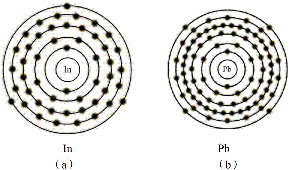
[0085] Such as figure 1 As shown, the electronic structure of Pb is 1s 2 2s 2 p 6 3s 2 p 6 d 10 4s 2 p 6 d 10 f 14 5s 2 p 6 d 10 6s 2 p 2 , the ionic radius is The electronic structure of In is 1s 2 2s 2 p 6 3s 2 p 6 d 10 4s ...

Embodiment 3

[0088] According to the preset mass ratio of 228:97:81, the particle size is in the range of 0.1μm-500μm, and the purity is greater than 99.99% of Tl 2 o 3 Powder, Ge 2 o 3 powder and ZnO powder into the ball mill; then, stir the powders added into the ball mill to obtain mixed powder, wherein the stirring time range is preferably 3h, and the stirring speed range is preferably 2000rpm; then, use phenolic resin type of binder, cold-pressed in the range of 100MPa-150MPa, and sintered at 1300°C-1700°C for 4 hours-9 hours in an aerobic atmosphere to form a target blank, and finally, the target The blank is machined, polished, and surface smoothed to obtain a chemical formula TlGeZnO 4 Target materials in atomic ratios indicated.

[0089] Such as Figure 4 As shown, the electronic structure of Tl is 1s 2 2s 2 p 6 3s 2 p 6 d 10 4s 2 p 6 d 10 f 14 5s 2 p 6 d 10 6s 2 p 1 , the ionic radius is The electronic structure of In is 1s 2 2s 2 p 6 3s 2 p 6 d 10 4s ...


PUM

PropertyMeasurementUnit
thicknessaaaaaaaaaa

Abstract

The embodiment of the invention discloses a target material and a preparation method thereof as well as a display device for forming a channel layer by utilizing the target material. The target material has an atom ratio as shown in a formula (I): AaBbGecZnOd (I), wherein A and B are respectively any one of Pb, Tl, Sn, Sb and Bi; the value ranges of a and b are both 0-100, comprise an end point value and are 0 when a and b are different; the value range of c is 0.01-100 and comprises the end point value. The target material provided by the embodiment of the invention is high in carrier mobility rate, can meet current requirements of an active display device of a high-resolution narrow-bezel integrated drive, and is low in cost.

Description

technical field [0001] The invention relates to the technical field of liquid crystal display, in particular to a target material, a preparation method thereof and a display device. Background technique [0002] Active display devices (such as active matrix liquid crystal display AM LCD and active matrix organic light-emitting diode AMOLED) have the advantages of low power consumption, excellent display quality, and long service life, so they are applied in more and more fields. The thin film transistor (TFT for short) is the core component of the active display device, controlling the switch of each pixel in the active display device. [0003] Thin film transistors in the prior art mainly include three kinds of amorphous silicon (a-Si) TFTs, low temperature polysilicon TFTs and oxide TFTs. Among them, amorphous silicon (a-Si) thin film transistors have been widely used in active matrix liquid crystal display AM LCD due to their advantages of large area uniformity, low manu...

Claims


Application Information

Patent Timeline
Patent Type & Authority Patents(China)
IPC IPC(8): C23C14/34
Inventor 何剑苏君海张色冯柯贤军周晓峰林宏信李建华
Owner TRULY SEMICON
Why Eureka
Try Eureka