Variable crucible ratio monocrystal silicon growth method

A growth method, single crystal silicon technology, applied in the direction of single crystal growth, single crystal growth, crystal growth, etc., can solve problems affecting device alignment and consistency, secondary defects, and insignificant gettering effect, etc., to achieve Strong compatibility, good axial uniformity, and easy industrialization

Active Publication Date: 2013-09-18
ZHEJIANG COWIN ELECTRONICS
View PDF8 Cites 3 Cited by
  • Summary
  • Abstract
  • Description
  • Claims
  • Application Information

AI Technical Summary

Problems solved by technology

If the oxygen content is too high, it will easily induce secondary defects, and if the oxygen concentration is too low, the internal gettering effect will not be obvious.
Silicon wafers with different oxygen concentrations have certain differences in device characteristics due to internal gettering effects and inconsistencies in the induced defects during the device manufacturing process, which affects the alignment and consistency of device manufacturing

Method used


Image

  • Variable crucible ratio monocrystal silicon growth method
  • Variable crucible ratio monocrystal silicon growth method

Examples


Embodiment 1

[0020] CG6000 single crystal furnace is adopted, with 16-inch thermal field, 25kg polycrystalline material, the target resistivity of the drawn monocrystalline silicon head is 35 ohm cm, the type of monocrystalline silicon is N type, and the size of monocrystalline silicon is 4 inches. A constant pressure of 40 torr, an argon gas flow rate of 40 slpm, a crucible rotation speed of 5 rpm, and a crystal rotation speed of 12 rpm were adopted.

[0021] Specific steps are as follows:

[0022] (1) Clean the thermal field, single crystal furnace, and quartz crucible;

[0023] (2) Carefully put the polycrystal and dopant into the quartz crucible;

[0024] (3) Close the single crystal furnace, flush the single crystal furnace with argon several times and evacuate it, and check the vacuum leak rate;

[0025] (4) Turn on the argon gas flow, turn on the heater to heat up, and melt the polysilicon;

[0026] (5) After the polycrystal is completely melted, reduce the power of the heater an...

Embodiment 2

[0033] CG6000 single crystal furnace is adopted, with 16-inch thermal field, 30kg polycrystalline material, the target resistivity of the drawn monocrystalline silicon head is 50 ohm cm, the type of monocrystalline silicon is N type, and the size of monocrystalline silicon is 5 inches. A constant pressure of 35 torr, an argon gas flow rate of 50 slpm, a crucible rotation speed of 6 rpm, and a crystal rotation speed of 14 rpm were adopted.

[0034] Specific steps are as follows:

[0035] (1) Clean the thermal field, single crystal furnace, and quartz crucible;

[0036] (2) Carefully put the polycrystal and dopant into the quartz crucible;

[0037] (3) Close the single crystal furnace, flush the single crystal furnace with argon several times and evacuate it, and check the vacuum leak rate;

[0038] (4) Turn on the argon gas flow, turn on the heater to heat up, and melt the polysilicon;

[0039] (5) After the polycrystal is completely melted, reduce the power of the heater an...


PUM


Abstract

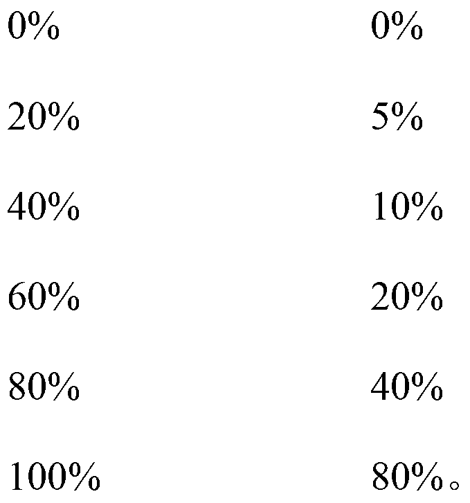
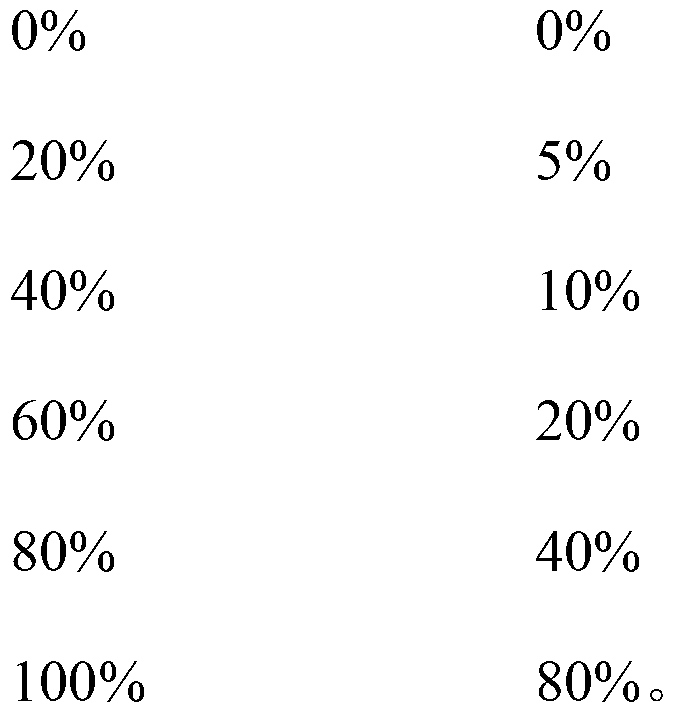
The invention discloses a variable crucible ratio monocrystal silicon growth method which comprises the following steps of: growing monocrystal silicon in a crucible; and after the monocrystal silicon enters constant-diameter growth, regulating variable crucible ratio to continuously increase so as to carry out variable crucible ratio monocrystal silicon growth. According to the variable crucible ratio monocrystal silicon growth method disclosed by the invention, the liquid level of monocrystal interface growth can be slowly increased, the natural thermal convection of a molten mass can be effectively accelerated, the oxygen content concentration of the molten mass can be kept and the axial oxygen content consistency of monocrystal silicon can be effectively improved; and the variable crucible ratio monocrystal silicon growth method is convenient to operate and suitable for the industrialized production.

Description

technical field [0001] The invention relates to the field of single crystal silicon chip processing and manufacturing, in particular to a method for growing single crystal silicon. Background technique [0002] The Czochralski single crystal growth method, also known as the Czochralski method, referred to as the CZ method, is to put high-purity polysilicon in a quartz crucible, heat it at a high temperature to melt it, and then use the seed crystal and rotary pulling method to achieve crystal growth through seeding and shouldering. , shoulder turning, equal diameter, finishing and other steps to gradually grow monocrystalline silicon. Because a quartz crucible is used in the process, the quartz crucible reacts with molten silicon at high temperature: Si+SiO 2 =2SiO, the generated SiO enters the molten silicon. Oxygen impurities are inevitably introduced during the crystal growth process. [0003] Oxygen impurities in silicon are easy to agglomerate and form oxygen precipi...

Claims


Application Information

Patent Timeline
Patent Type & Authority Applications(China)
IPC IPC(8): C30B15/20C30B29/06
Inventor 孙新利
Owner ZHEJIANG COWIN ELECTRONICS
Why Eureka
Try Eureka