Graphene/silicon solar cell and manufacturing method thereof

A silicon solar cell and graphene technology, applied in the field of solar energy, to achieve the effect of reducing series resistance, increasing output power and increasing open circuit voltage

Active Publication Date: 2013-09-18
ZHEJIANG UNIV
View PDF3 Cites 9 Cited by
  • Summary
  • Abstract
  • Description
  • Claims
  • Application Information

AI Technical Summary

Problems solved by technology

[0004] As mentioned earlier, the research on the application of graphene materials in solar cells has not yet achieved progress comparable to the current industrialization technology of solar cells

Method used


Image

  • Graphene/silicon solar cell and manufacturing method thereof
  • Graphene/silicon solar cell and manufacturing method thereof

Examples


Embodiment 1

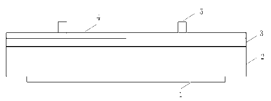
[0023] 1) Immerse the p-type monocrystalline silicon wafer in a NaOH alkali solution with a mass concentration of 3% to form a textured structure on the surface of the p-type silicon layer;

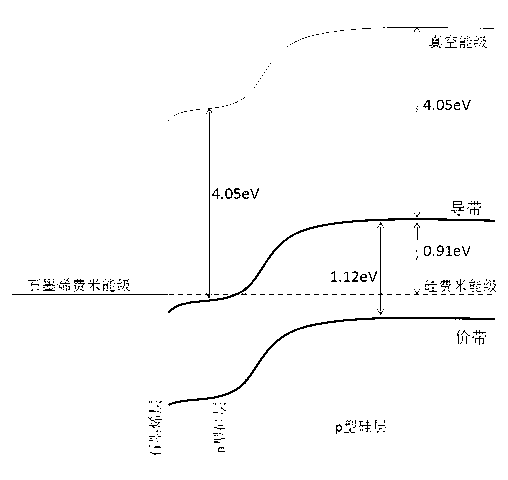
[0024] 2) Put the textured sample into a diffusion furnace for phosphorus diffusion to form an n-type silicon layer. The diffusion temperature is 850°C and the surface doping concentration is 10 18 cm -3 , the junction depth is 0.2μm;

[0025] 3) Use laser etching to remove the edge doped layer;

[0026] 4) Transfer the n-type doped graphene to the phosphorus-doped n-type silicon layer, the graphene doping concentration is 10 12 cm -2 ;

[0027] 5) Print Ag and Al paste on the back of the p-type silicon layer and dry it, print Ag paste on the n-type doped graphene, and then put it into a belt sintering furnace for sintering, the sintering temperature is 950°C, and the time is 1min. The back electrode and the front electrode are fabricated to obtain a graphene / silicon solar cell.

Embodiment 2

[0029] 1) Immerse the p-type polysilicon wafer in HF / HNO 3 Etching in a mixed solution with a volume ratio of 3:1 to form a suede on the surface of the p-type silicon layer;

[0030] 2) Put the textured sample into a diffusion furnace for phosphorous diffusion to form an n-type silicon layer, the diffusion temperature is 900°C, and the surface doping concentration is 10 21 cm -3 , the junction depth is 0.4μm;

[0031] 3) Plasma etching is used to remove the edge doped layer;

[0032] 4) Transfer the n-type doped graphene to the phosphorus-doped n-type silicon layer, the graphene doping concentration is 2×10 13 cm -2 ;

[0033] 5) Print Ag and Al paste on the back of the p-type silicon layer and dry it, print Ag paste on the n-type doped graphene, and then put it into a belt sintering furnace for sintering, the sintering temperature is 850°C, and the time is 3min. The back electrode and the front electrode are fabricated to obtain a graphene / silicon solar cell.

Embodiment 3

[0035] 1) Immerse the p-type monocrystalline silicon wafer in a NaOH alkali solution with a mass concentration of 2%, so that the surface of the p-type silicon layer forms a textured structure;

[0036] 2) Phosphorus ion implantation was performed on the textured sample to form an n-type silicon layer with a surface doping concentration of 10 19 cm -3 , the junction depth is 0.6μm;

[0037] 3) Laser etching is used to remove the edge doped layer;

[0038] 4) Transfer the n-type doped graphene to the phosphorus-doped n-type silicon layer, the graphene doping concentration is 5×10 12 cm -2 ;

[0039] 5) Thermally evaporate the aluminum electrode on the back of the p-type silicon layer, thermally evaporate the gold electrode on the n-type doped graphene, and then put it into a belt sintering furnace for sintering. The sintering temperature is 400°C and the time is 30min. The back electrode and the front electrode After the fabrication is completed, a graphene / silicon solar ...


PUM


Abstract

The invention relates to a grapheme/silicon solar cell and a manufacturing method thereof. The grapheme/silicon solar cell sequentially comprises a back electrode, a p-type silicon layer, an n-type silicon layer, an n-type doped grapheme layer and a front electrode from bottom up, wherein the grapheme doped carrier concentration is no less than 10 (12) cm (-2). The manufacturing method thereof comprises firstly immersing a p-type silicon wafer into chemical texturing solution to enable the surface of the p-type silicon wafer to form a texturing structure; secondly, leading a textured sample to be subjected to phosphor doping through phosphorus diffusion or phosphorus ion implantation to form the n-type silicon layer; thirdly, transferring the n-type doped grapheme layer to the phosphor-doped n-type silicon layer; fourthly, manufacturing the back electrode on the p-type silicon layer; and lastly, manufacturing the front surface electrode on the n-type doped grapheme layer. According to the grapheme/silicon solar cell, the grapheme materials are utilized, so that the open-circuit voltage of the solar cell is improved, the series resistance of the solar cell is reduced, and the output power is improved.

Description

technical field [0001] The invention relates to a solar cell and a manufacturing method thereof, in particular to a graphene / silicon solar cell and a manufacturing method thereof, and belongs to the technical field of solar energy. Background technique [0002] In recent years, solar cells, as a new type of green energy, are playing an increasingly important role in the sustainable development of human beings. Among them, silicon-based solar cells, especially crystalline silicon solar cells, account for ~90% of the market. However, compared with conventional power generation, the cost of solar cell power generation is still high, which limits the large-area application. One of the reasons for the high cost of solar cell power generation is the high cost of cell manufacturing, and another major reason is its low photoelectric conversion efficiency. [0003] Since graphene materials were first stably prepared in 2004, more and more studies have found that graphene materials ...

Claims


Application Information

Patent Timeline
Patent Type & Authority Applications(China)
IPC IPC(8): H01L31/0216H01L31/0224H01L31/068H01L31/18
CPCY02E10/547Y02P70/50
Inventor 林时胜李晓强
Owner ZHEJIANG UNIV
Why Eureka
Try Eureka