Supercharge Your Innovation With Domain-Expert AI Agents!

Group 13 nitride crystal and group 13 nitride crystal substrate

A technology of nitride crystals and grain boundaries, applied in the fields of nitrogen compounds, crystal growth, chemical instruments and methods, etc., can solve problems such as difficulty in providing high-quality bulk

Inactive Publication Date: 2013-09-25
RICOH KK
View PDF11 Cites 8 Cited by
  • Summary
  • Abstract
  • Description
  • Claims
  • Application Information

AI Technical Summary

Problems solved by technology

[0011] However, in conventional techniques, it is difficult to provide high-quality bulk (bulk) crystals due to the influence of c-plane threading dislocations (threading dislocation) and basal plane dislocations.

Method used


Image

  • Group 13 nitride crystal and group 13 nitride crystal substrate
  • Group 13 nitride crystal and group 13 nitride crystal substrate
  • Group 13 nitride crystal and group 13 nitride crystal substrate

Examples


Embodiment

[0249] Although Examples will be described below to illustrate the present invention in more detail, the Examples are not intended to limit the present invention. Reference numerals correspond to those in the reference Figure 11 and Figure 12 Those in the configuration of the crystal fabrication apparatuses 1 and 2 described.

[0250] Seed crystal production

[0251] A seed crystal for production of a Group 13 nitride crystal was produced by the following production method.

manufacture Embodiment 1

[0253] use Figure 11 The crystal manufacturing apparatus 1 shown in produces a seed crystal of the first region 21A.

[0254] Gallium with a nominal purity of 99.99999% and sodium with a nominal purity of 99.95% were fed in a molar ratio of 0.25:0.75 into a reaction vessel 12 made of a BN sintered body with an inner diameter of 92 mm.

[0255] The reaction vessel 12 was placed in the pressure-resistant vessel 11 under a high-purity Ar gas atmosphere in a glove box. Subsequently, the valve 31 was closed to isolate the inside of the reaction vessel 12 from the external atmosphere, and the pressure-resistant vessel 11 was sealed in such a manner as to be filled with Ar gas.

[0256] Subsequently, the pressure-resistant container 11 was taken out from the glove box and incorporated into the crystal manufacturing apparatus 1 . In other words, the pressure-resistant container 11 is placed at a predetermined position with respect to the heater 13 and connected to the valve for N a...

manufacture Embodiment 2

[0262] Crystal growth was performed in the same manner as in Production Example 1 of the seed crystal, except for the following conditions: alumina was used as the material of the reaction vessel 12; a plate made of a BN sintered body fitted into the bottom surface of the reaction vessel 12 was placed ; put N 2 The partial pressure at the crystal growth temperature of 870° C. in the pressure vessel 11 is maintained at 6 MPa (N 2 The partial pressure at room temperature in the pressure-resistant vessel 11 was 2.8 MPa); and the crystal growth time was set to 300 hours.

[0263] As a result, similarly to Production Example 1 of the seed crystal, it was found that a large amount of colorless and transparent seed crystal 30 , which is a grown GaN crystal, grew. The crystal diameter d of the seed crystal 30 is about 100-500 μm, the length L thereof is about 10-15 mm, and the ratio L / d of the length L to the crystal diameter d is about 30-500.


PUM

PropertyMeasurementUnit
thicknessaaaaaaaaaa
thicknessaaaaaaaaaa
heightaaaaaaaaaa

Abstract

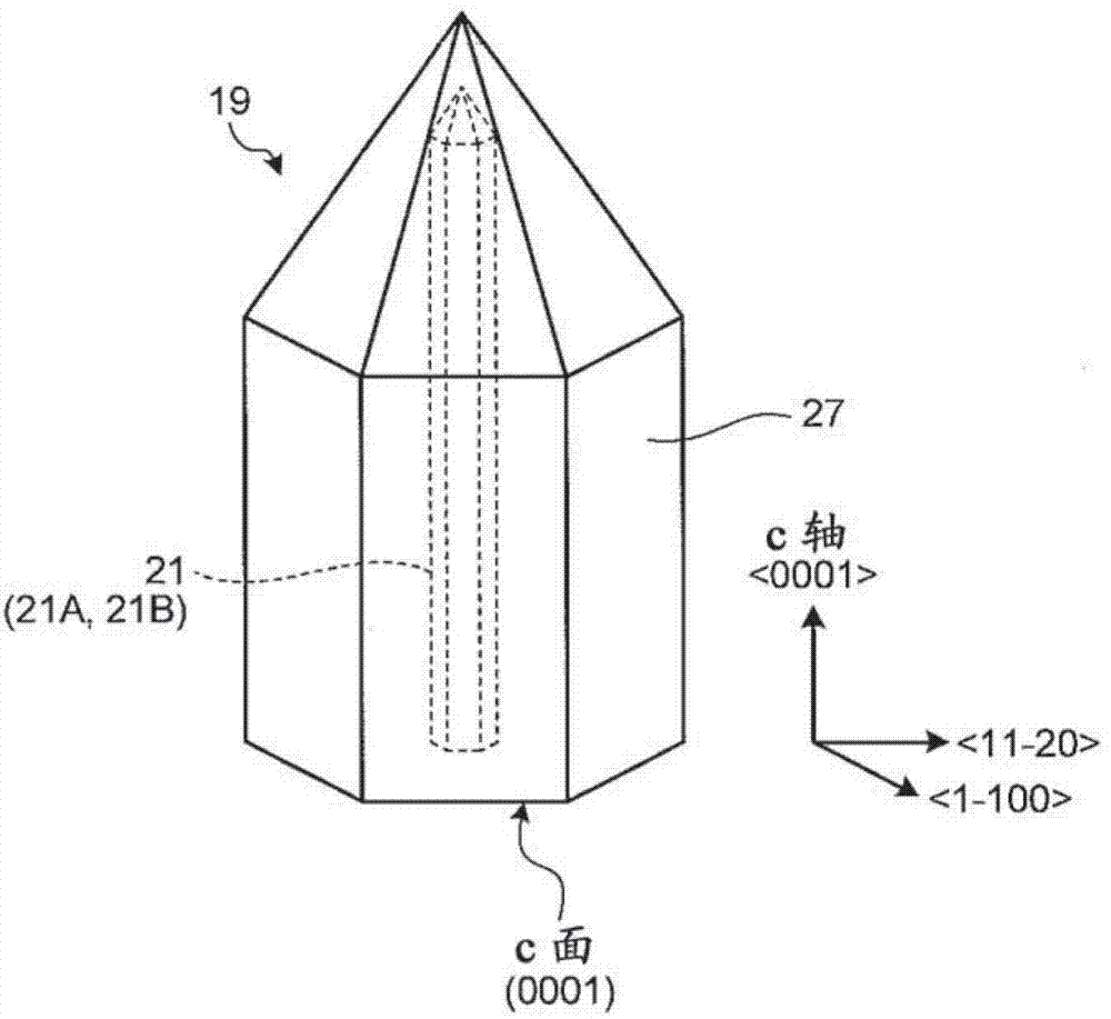
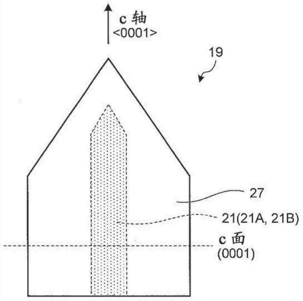
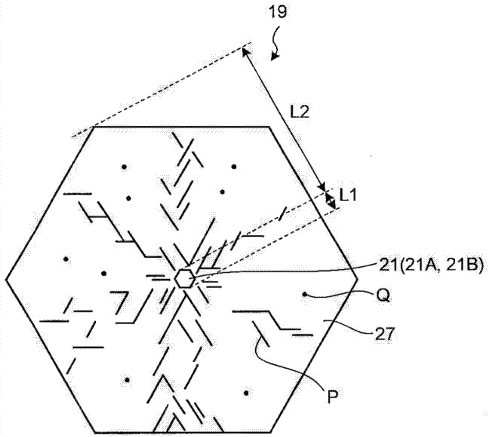
A group 13 nitride crystal has a hexagonal crystal structure containing a nitrogen atom and at least one type of metal atom selected from the group consisting of B, Al, Ga, In, and Tl. The group 13 nitride crystal has a basal plane dislocation in a plurality of directions. Dislocation density of the basal plane dislocation is higher than dislocation density of a threading dislocation of a c-plane.

Description

technical field [0001] The present invention relates to a Group 13 nitride crystal and a Group 13 nitride crystal substrate (substrate). Background technique [0002] Gallium nitride (GaN) based semiconductor materials are used in semiconductor devices such as blue light emitting diodes (LEDs), white LEDs and laser diodes (LDs). White LEDs are used, for example, in the backlighting of mobile phone screens and liquid crystal displays and for lighting. Blue LEDs are used, for example, in traffic lights and other lighting. A blue-violet LD is used as a light source for Blu-ray discs. Today, most GaN-based semiconductor devices used as UV, violet-blue-green light sources are fabricated on sapphire or silicon carbide (SiC) substrates using, for example, metal-organic chemical vapor deposition (MOCVD) or molecular beam epitaxy (MBE) Manufactured by crystal growth. [0003] If sapphire or SiC is used as a substrate, crystal defects increase due to large differences in thermal e...

Claims


Application Information

Patent Timeline
Patent Type & Authority Applications(China)
IPC IPC(8): C30B29/40
CPCC01B21/0632C01B21/064C30B9/06C30B29/403C30B29/406C30B29/06C30B29/38
Inventor 林昌弘皿山正二佐藤隆木村千春三好直哉村上明繁和田纯一
Owner RICOH KK
Features
  • R&D
  • Intellectual Property
  • Life Sciences
  • Materials
  • Tech Scout
  • Unparalleled Data Quality
  • Higher Quality Content
  • 60% Fewer Hallucinations
Learn More