Oxide semiconductor thin film and thin film transistor

An oxide semiconductor and thin film transistor technology, applied in transistors and other directions, can solve the problems of high conductivity and inability to obtain oxygen, and achieve the effects of high electron mobility, increased photostability, and high anti-aging properties.

Active Publication Date: 2013-09-25
SOUTH CHINA UNIV OF TECH
View PDF3 Cites 8 Cited by
  • Summary
  • Abstract
  • Description
  • Claims
  • Application Information

AI Technical Summary

Problems solved by technology

If annealed in nitrogen or inert gas, it will cause high conductivity because oxygen cannot be obtained

Method used


Image

  • Oxide semiconductor thin film and thin film transistor
  • Oxide semiconductor thin film and thin film transistor
  • Oxide semiconductor thin film and thin film transistor

Examples


Embodiment 1

[0033] An oxide semiconductor thin film, the composition of which is M 2x In 2-2x o 3-δ And the composition does not include Zn and Sn, wherein M is a group IIIB element in the periodic table of elements, 0.001≤x≤0.3, 0≤δ<3.

[0034] The composition of the oxide semiconductor thin film includes group IIIB elements and In, and does not contain Zn and Sn in the composition, and is based on In 2 o 3 A semiconductor thin film prepared as a matrix material. The matrix material refers to the material that accounts for the main component of the compound. The carrier concentration of the oxide semiconductor thin film is less than 5×10 19 cm -3 , the carrier concentration is preferably less than 10 17 cm -3 .

[0035] The radius of the In atom is larger than that of the Zn atom, and its 5s orbitals can overlap, which has a high electron mobility. At the same time, an important property of the In atom is that it can form an electron channel even in the amorphous state. Therefor...

Embodiment 2

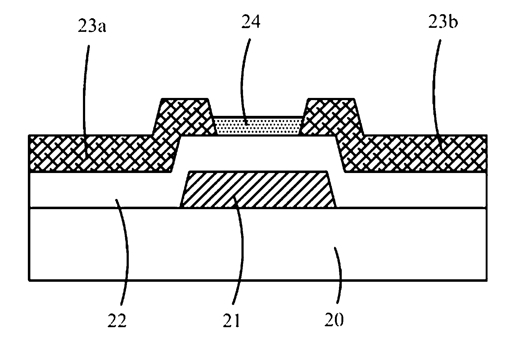
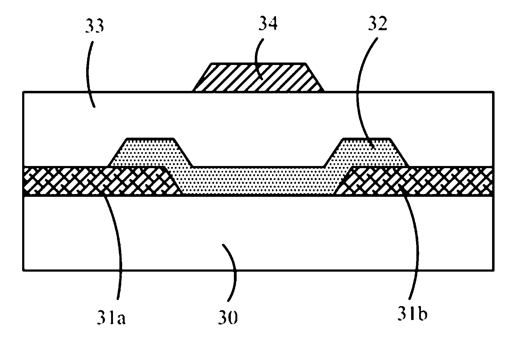
[0051] A thin film transistor, comprising: a gate, a channel layer, an insulating layer between the gate and the channel layer, and a source and a drain electrically connected to both ends of the channel layer; the material of the channel layer is The oxide semiconductor thin film of Example 1. The electrical connection means that there is a conductive channel between the two, the two can be in direct contact, and a buffer layer can be further included.

[0052] It should be noted that, the specific structure of the thin film transistor can adopt thin film transistors of different structure types. As long as the channel material is the material of Embodiment 1, it all belongs to the technology of the present invention.

[0053] In the thin film transistor of the present invention, since the oxide thin film transistor used as the channel layer can effectively control the quantity of oxygen vacancies, the performance of the prepared thin film transistor is stable.

[0054] Bec...

Embodiment 3

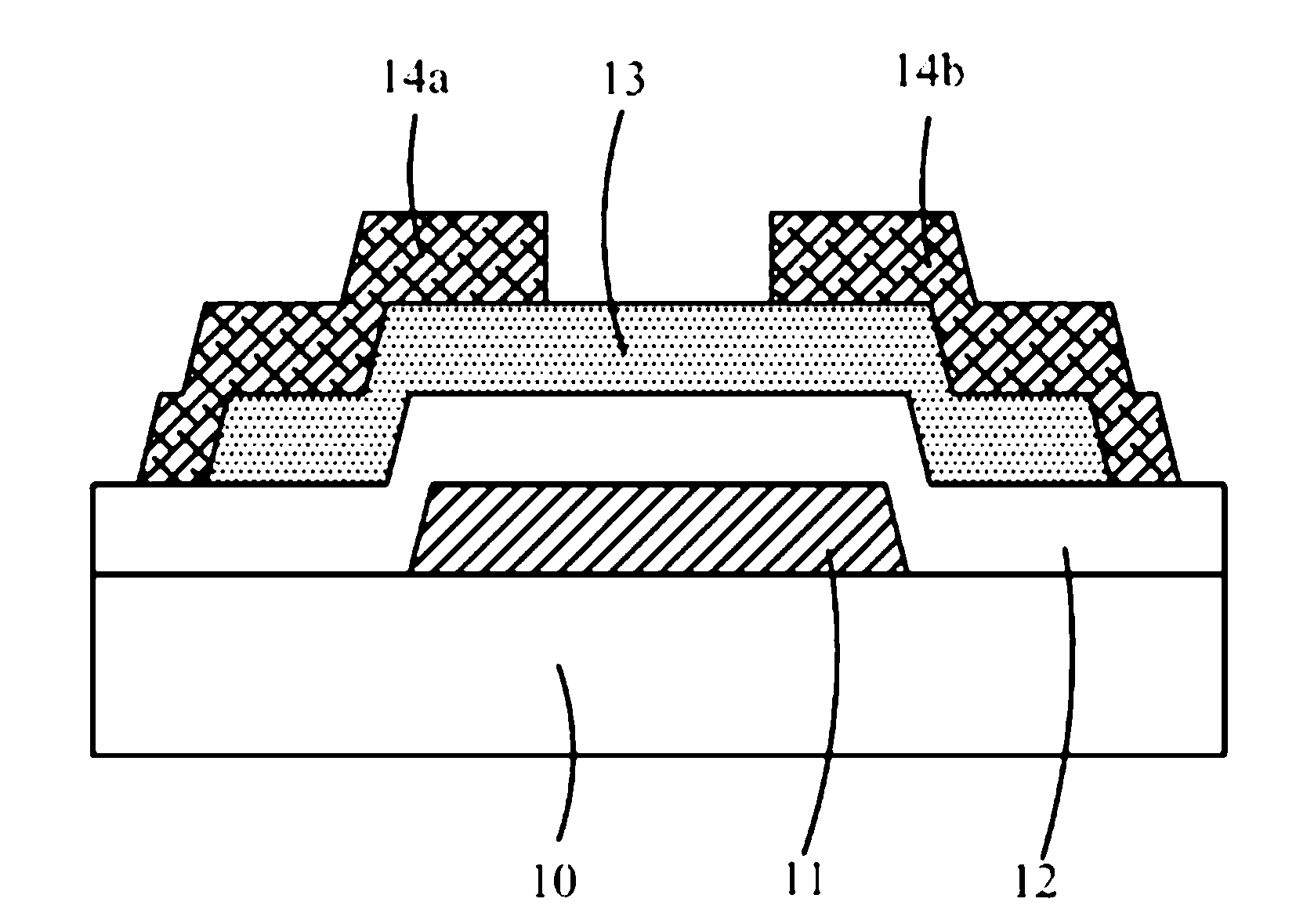
[0057] A thin film transistor with a bottom-gate top-contact structure, such as figure 1 As shown, it is provided with: a substrate 10, a gate 11 located on the substrate 10, an insulating layer 12 located on the substrate 10 and the gate 11, a channel layer covering the upper surface of the insulating layer 12 and corresponding to the gate 11 13 , and a source 14 a and a drain 14 b that are spaced apart from each other and electrically connected to both ends of the channel layer 13 .

[0058] It should be noted that for the thin film transistor, an etching stopper layer can be further provided on the channel layer 13 according to specific needs.

[0059] The substrate 10 may be one of substrate materials such as glass, flexible polymer substrate, silicon wafer, metal foil, and quartz, and may further include a buffer layer or a water-oxygen barrier layer covering the substrate.

[0060] The material of the gate 11 can be a conductive material, such as metal, alloy, conductiv...


PUM

PropertyMeasurementUnit
thicknessaaaaaaaaaa
thicknessaaaaaaaaaa
thicknessaaaaaaaaaa

Abstract

The invention provides an oxide semiconductor thin film and a thin film transistor. The composition of the oxide semiconductor thin film is M[2x]In[2-2x]O[3-delta], wherein M is a III B family element, x is larger than or equal to 0.001 and small than or equal to 0.3, and delta is larger than or equal to 0 and small than 3. The III B family element is one or more arbitrary elements in a group consisting of Sc, Y, Ac, La, Ce, Pr, Nd, Pm, Sm, Eu, Gd, Tb, Dy, Ho, Er, Tm, Yb, and Lu. The thickness of the thin film is 5nm to 200nm. The carrier concentration of the oxide semiconductor thin film is less than 5*10<19>cm<-3>. The oxide semiconductor thin film is used as a channel layer material of the thin film transistor. The thin film transistor is provided with a gate, a channel layer, an insulated layer between the gate and the channel layer, a source electrode and a drain electrode, and the source electrode and the drain electrode are respectively connected to two ends of the channel layer. The channel layer is provided with the above oxide semiconductor thin film. The oxide semiconductor thin film and the oxide semiconductor thin film have the advantages of good performance, simple preparation and wide adaptation range.

Description

technical field [0001] The invention belongs to the field of semiconductor materials and devices, in particular to an oxide semiconductor thin film and a thin film transistor using the oxide semiconductor thin film as a channel layer material. Background technique [0002] In recent years, thin film transistors (TFT, Thin Film Transistor) based on oxide semiconductors have received more and more attention in the field of flat panel displays, especially in the field of organic electroluminescent displays (OLEDs). [0003] At present, the material of the semiconductor channel layer of the thin film transistor used for flat panel display is mainly silicon material, including amorphous silicon (a-Si: H), polycrystalline silicon, microcrystalline silicon and the like. However, amorphous silicon thin film transistors are sensitive to light and have low mobility (<1cm 2 / Vs) and poor stability; although polysilicon thin film transistors have high mobility, their electrical unif...

Claims


Application Information

Patent Timeline
Patent Type & Authority Applications(China)
IPC IPC(8): H01L29/786
Inventor 兰林锋彭俊彪林振国
Owner SOUTH CHINA UNIV OF TECH
Why Eureka
Try Eureka